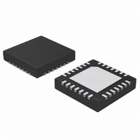
ATA5278-PKQI Atmel, ATA5278-PKQI Datasheet - Page 15

ATA5278-PKQI
Manufacturer Part Number
ATA5278-PKQI
Description
IC ANTENNA DVR STAND-ALONE 28QFN
Manufacturer
Atmel
Type
Stand Alone Antenna Driverr
Datasheet
1.ATA5278-PKQI.pdf
(34 pages)
Specifications of ATA5278-PKQI
Rf Type
TPM
Frequency
125kHz
Package / Case
28-VFQFN
Maximum Operating Temperature
+ 105 C
Mounting Style
SMD/SMT
Minimum Operating Temperature
- 40 C
Lead Free Status / RoHS Status
Lead free / RoHS Compliant
Features
-
Lead Free Status / Rohs Status
Lead free / RoHS Compliant
Other names
ATA5278-PKQITR
3.11
4832D–RKE–12/07
QSC Feature
The carrier signal is now always on as long as the LF data is in the buffer. It is only at the change
of the LF data values that the phase of the antenna current is shifted by 180°. For further details,
please refer to the section
An internal timer, derived from the system clock generates the modulation times for the half bits
applied to the driver stage. These times depend on the selected LF baud rate in configuration
register 2 (i.e., the bits BR0 and BR1).
timings.
Table 3-2.
Note that due to synchronization issues, the time for which the LF field is really active in ASK
mode when transmitting one half bit might vary by ±8 µs. This is a non-accumulating effect,
which means, the transmission time for the complete LF data stream may also vary by ±8 µs,
independent of the total amount of logical bits. The same is true for the distance of two phase
shifts when transmitting LF data in PSK mode.
If data rates above 2 kbauds are demanded or the PSK modulation mode is selected, the use of
an external antenna current loop switch is mandatory. This switch has to be controlled in a
defined way which is supported by the ATA5278. For further details on this topic, please refer to
the section
The Quick Start Control (QSC) feature supports a short oscillation build up and decay time dur-
ing LF data modulation. An external high-voltage MOS transistor is used as a switch to close
and open the current loop of the antenna. By synchronizing this switch to the zero-crossing
events of the antenna current, very short build-up and decay times for the LF field, and therefore
high data rates can be achieved.
Figure 3-11. QSC Operation
Half bit from
BR0 Bit
data buffer
Setting
Voltage at
QSC pin
antenna
through
Current
0
1
0
1
“QSC Feature”
LF Baud Rate Time Values
BR1 Bit
Setting
0
0
1
1
Modulation in ASK mode
“Driver Stage” on page
.
Baud Rate
Selected
1 kbaud
2 kbaud
3 kbaud
4 kbaud
Table 3-2
16.
Time for One
lists the bit settings and their corresponding
t
Half Bit
Bitlength
512 µs
256 µs
160 µs
128 µs
/2
Modulation in PSK mode
Time for One Logical Bit
ATA5278
1024 µs
t
512 µs
320 µs
256 µs
Bitlength
15


