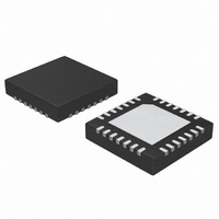
ATA5278-PKQI Atmel, ATA5278-PKQI Datasheet - Page 24

ATA5278-PKQI
Manufacturer Part Number
ATA5278-PKQI
Description
IC ANTENNA DVR STAND-ALONE 28QFN
Manufacturer
Atmel
Type
Stand Alone Antenna Driverr
Datasheet
1.ATA5278-PKQI.pdf
(34 pages)
Specifications of ATA5278-PKQI
Rf Type
TPM
Frequency
125kHz
Package / Case
28-VFQFN
Maximum Operating Temperature
+ 105 C
Mounting Style
SMD/SMT
Minimum Operating Temperature
- 40 C
Lead Free Status / RoHS Status
Lead free / RoHS Compliant
Features
-
Lead Free Status / Rohs Status
Lead free / RoHS Compliant
Other names
ATA5278-PKQITR
24
ATA5278
Note that in any case, the test pins SCANE and TEST must be connected to ground. These pins
are for factory test purposes only. For safety reasons, these pins are equipped with a pull-down
structure, so that the signals are still defined in case of broken connections. Connecting them to
any signal other than ground will result in malfunctions which can lead to the destruction of the
chip or the external components.
The power dissipation of ATA5278 is, as already noted, dependant of the supply voltage and the
selected antenna current. Assuming an antenna with maximum allowable impedance (i.e., the
boost converter will generate 40V output voltage) and the maximum available output current
selected (i.e., step 16), the power dissipation of ATA5278 results as shown in
page 24
Figure 3-17. Power Dissipation versus Supply Voltage
The static thermal resistance of the chip, soldered onto a PCB can hardly be lowered beneath
30 K/W. Hence, a static operation of ATA5278 is not possible in all cases. But as most applica-
tions require only a temporary LF field, the dynamic thermal effects (i.e., the thermal
capacitances) are important parameters that must be taken into account.
Figure 3-18 on page 25
design.
• The ground pin of R
as possible. The same is true for the connection between L1, D2 and VL1..3 and the
connection between D2, the positive pin of C4 and the VDS pin.
SHUNT
8
7
6
5
4
3
2
1
shows the maximum reachable LF carrier duration for an example PCB
7.5
, C2, C4 and the AGND pin should be connected together as closely
8.5
Ta = 85
Ta = 105
9.5
˚
C
Voltage at VBATT pin (V)
˚
C
10.5
11.5
12.5
13.5
14.5
15.5
16.5
Figure 3-17 on
4832D–RKE–12/07


