APT100GT120JRDL Microsemi Power Products Group, APT100GT120JRDL Datasheet - Page 2
APT100GT120JRDL
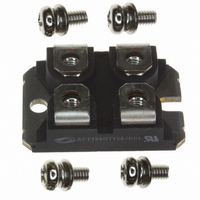
Manufacturer Part Number
APT100GT120JRDL
Description
IGBT 1200V 123A 570W SOT227
Manufacturer
Microsemi Power Products Group
Datasheet
1.APT100GT120JRDL.pdf
(9 pages)
Specifications of APT100GT120JRDL
Igbt Type
NPT
Configuration
Single
Voltage - Collector Emitter Breakdown (max)
1200V
Vce(on) (max) @ Vge, Ic
3.7V @ 15V, 100A
Current - Collector (ic) (max)
123A
Current - Collector Cutoff (max)
300µA
Input Capacitance (cies) @ Vce
6.7nF @ 25V
Power - Max
570W
Input
Standard
Ntc Thermistor
No
Mounting Type
Chassis Mount
Package / Case
ISOTOP
Lead Free Status / RoHS Status
Lead free / RoHS Compliant
Other names
APT100GT120JRDLMI
APT100GT120JRDLMI
APT100GT120JRDLMI


Dynamic Characteristic
Thermal and Mechanical Characteristics
1 Repetitive Rating: Pulse width limited by maximum junction temperature.
2 For Combi devices, I
3 See MIL-STD-750 Method 3471.
4 E
5 E
6 E
7 R
Microsemi reserves the right to change, without notice, the specifi cations and information contained herein.
Symbol
Symbol Characteristic / Test Conditions
SSOA
V
z a the IGBT turn-on loss. Tested in inductive switching test circuit shown in fi gure 21, but with a Silicon Carbide diode.
loss. (See Figures 21, 22.)
V
t
t
t
t
E
E
E
E
C
C
C
Q
Q
R
R
d(on)
d(off)
E
d(on)
d(off)
E
Isolation
Q
on1
on2
off
G
W
GEP
t
t
on1
on2
t
t
on1
on2
oes
res
θ
θ
ies
ge
off
off
gc
r
f
r
f
g
is external gate resistance not including gate driver impedance.
JC
JC
is the clamped inductive turn-off energy measured in accordance with JEDEC standard JESD24-1. (See Figures 21, 23.)
T
is the clamped inductive turn-on energy of the IGBT only, without the effect of a commutating diode reverse recovery current adding to
is the clamped inductive turn-on energy that includes a commutating diode reverse recovery current in the IGBT turn-on switching
Characteristic
Input Capacitance
Output Capacitance
Reverse Transfer Capacitance
Gate-to-Emitter Plateau Voltage
Total Gate Charge
Gate-Emitter Charge
Gate-Collector Charge
Switching Safe Operating Area
Turn-On Delay Time
Current Rise Time
Turn-Off Delay Time
Current Fall Time
Turn-On Switching Energy
Turn-On Switching Energy
Turn-Off Switching Energy
Turn-On Delay Time
Current Rise Time
Turn-Off Delay Time
Current Fall Time
Turn-On Switching Energy
Turn-On Switching Energy
Turn-Off Switching Energy
Junction to Case (IGBT)
Junction to Case (DIODE)
Package Weight
RMS Voltage
ces
includes both IGBT and FRED leakages.
(50-60Hz Sinusoidal Waveform from Terminals to Mounting Base for 1 Min.)
6
6
4
4
5
5
T
J
= 150°C, R
Inductive Switching (125°C)
Inductive Switching (25°C)
L = 100μH, V
V
GE
Test Conditions
Gate Charge
= 0V, V
V
T
V
T
V
V
V
V
R
R
I
I
I
f = 1MHz
J
J
CC
CC
C
C
C
CE
G
GE
GE
GE
G
G
= +25°C
= 125°C
= 100A
= 100A
= 100A
= 1.0Ω
= 600V
= 4.7Ω
= 4.7Ω
= 800V
= 800V
= 15V
= 15V
= 15V
CE
CE
= 1200V
= 25V
7
, V
GE
= 15V,
2500
Min
200
Min
-
-
-
-
-
-
-
-
-
-
-
-
-
-
-
-
-
-
-
-
-
-
-
-
APT100GT120JRDL(G)
17600
22380
10950
6700
6530
4380
7240
TBD
TBD
10.0
Typ
685
400
100
630
100
710
75
50
36
50
37
29.2
Typ
-
-
-
Max
Max
0.22
0.80
-
-
-
-
-
-
-
-
-
-
-
-
-
-
-
-
-
-
-
-
-
-
-
Unit
°C/W
Unit
Volts
nC
pF
ns
μJ
ns
μJ
V
A
g
Related parts for APT100GT120JRDL
Image
Part Number
Description
Manufacturer
Datasheet
Request
R

Part Number:
Description:
IGBT 600V 100A 463W TO247
Manufacturer:
Microsemi Power Products Group
Datasheet:

Part Number:
Description:
IGBT 600V 198A 833W TO264
Manufacturer:
Microsemi Power Products Group
Datasheet:
Part Number:
Description:
IGBT 600V 41A 187W TO247
Manufacturer:
Microsemi Power Products Group
Datasheet:
Part Number:
Description:
MOSFET N-CH 600V 23A TO-247
Manufacturer:
Microsemi Power Products Group
Datasheet:

Part Number:
Description:
MOSFET N-CH 500V 17A TO-220
Manufacturer:
Microsemi Power Products Group
Datasheet:
Part Number:
Description:
MOSFET N-CH 1200V 3.5A TO-220
Manufacturer:
Microsemi Power Products Group
Datasheet:
Part Number:
Description:
MOSFET N-CH 500V 22A TO-247
Manufacturer:
Microsemi Power Products Group
Datasheet:
Part Number:
Description:
MOSFET N-CH 100V 75A TO-247
Manufacturer:
Microsemi Power Products Group
Datasheet:
Part Number:
Description:
MOSFET N-CH 200V 56A TO-247
Manufacturer:
Microsemi Power Products Group
Datasheet:
Part Number:
Description:
MOSFET N-CH 500V 27A TO-247
Manufacturer:
Microsemi Power Products Group
Datasheet:
Part Number:
Description:
MOSFET N-CH 300V 40A TO-247
Manufacturer:
Microsemi Power Products Group
Datasheet:
Part Number:
Description:
MOSFET N-CH 200V 59A TO-247
Manufacturer:
Microsemi Power Products Group
Datasheet:
Part Number:
Description:
MOSFET N-CH 500V 26A TO-247
Manufacturer:
Microsemi Power Products Group
Datasheet:
Part Number:
Description:
MOSFET N-CH 300V 40A TO-247
Manufacturer:
Microsemi Power Products Group
Datasheet:
Part Number:
Description:
MOSFET N-CH 200V 65A TO-247
Manufacturer:
Microsemi Power Products Group
Datasheet: