TFDU6103-TR3 Vishay, TFDU6103-TR3 Datasheet - Page 6
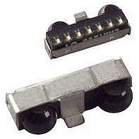
TFDU6103-TR3
Manufacturer Part Number
TFDU6103-TR3
Description
Infrared Transceivers SIR 115.2kbits Side View
Manufacturer
Vishay
Type
Fastr
Datasheet
1.TFDU6103-TR3.pdf
(13 pages)
Specifications of TFDU6103-TR3
Data Transmission Rate
4000 Kbits/s
Input Current
10 mA
Mounting Style
SMD/SMT
Power Dissipation
500 mW
Wavelength
886 nm
Continual Data Transmission
4 Mbit/s
Transmission Distance
1 m
Radiant Intensity
170 mW/sr
Half Intensity Angle Degrees
48 deg
Pulse Width
2.1 us
Maximum Rise Time
40 ns
Maximum Fall Time
40 ns
Led Supply Voltage
- 0.5 V to 6.5 V
Maximum Forward Current
10 mA
Operating Voltage
2.4 V to 5.5 V
Maximum Operating Temperature
+ 85 C
Minimum Operating Temperature
- 25 C
Dimensions
9.7 mm x 4.7 mm x 4 mm
Data Rate Max
4Mbps
Data Transmission Distance
1m
Peak Wavelength
886nm
Supply Current
2mA
Supply Voltage Range
2.4V To 5.5V
Operating Temperature Range
-25°C To +85°C
Msl
MSL 4 - 72 Hours
Data Rate
4Mbps
Angle Of Half Sensitivity
48°
Communication Distance
100
Package Type
Ultra Small Profile
Fall Time
40ns
Rise Time
40ns
Operating Supply Voltage (typ)
2.5/3.3/5V
Operating Supply Voltage (min)
2.4V
Operating Supply Voltage (max)
5.5V
Mounting
Surface Mount
Pin Count
8
Operating Temp Range
-25C to 85C
Operating Temperature Classification
Commercial
Idle Current, Typ @ 25° C
2mA
Link Range, Low Power
1m
Operating Temperature
-25°C ~ 85°C
Orientation
Side View
Shutdown
*
Size
9.7mm x 4.7mm x 4mm
Standards
IrPHY 1.4
Supply Voltage
2.4 V ~ 5.5 V
Lead Free Status / RoHS Status
Lead free / RoHS Compliant
Lead Free Status / RoHS Status
Lead free / RoHS Compliant, Lead free / RoHS Compliant
Available stocks
Company
Part Number
Manufacturer
Quantity
Price
Company:

Part Number:
TFDU6103-TR3
Manufacturer:
ST
Quantity:
1 001
Company:
Part Number:
TFDU6103-TR3
Manufacturer:
VISHAY
Quantity:
6 580


TFDU6103
Vishay Semiconductors
RECOMMENDED CIRCUIT DIAGRAM
Vishay Semiconductors transceivers integrate a sensitive
receiver and a built-in power driver. The combination of both
needs a careful circuit board layout. The use of thin, long,
resistive and inductive wiring should be avoided. The inputs
(TXD, SD) and the output RXD should be directly (DC)
coupled to the I/O circuit.
The capacitor C1 is buffering the supply voltage and reduces
the influence of the inductance of the power supply line. This
one should be a Tantalum or other fast capacitor to
guarantee the fast rise time of the IRED current. The resistor
R1 is only necessary for higher operating voltages and
I/O AND SOFTWARE
In the description, already different I/Os are mentioned.
Different combinations are tested and the function verified
with the special drivers available from the I/O suppliers. In
special cases refer to the I/O manual, the Vishay application
notes, or contact directly Vishay Sales, Marketing or
Application.
MODE SWITCHING
The TFDU6103 is in the SIR mode after power on as a
default mode, therefore the FIR data transfer rate has to be
set by a programming sequence using the TXD and SD
inputs as described below. The low frequency mode covers
speeds up to 115.2 kbit/s. Signals with higher data rates
should be detected in the high frequency mode. Lower
frequency data can also be received in the high frequency
mode but with reduced sensitivity.
To switch the transceivers from low frequency mode to the
high frequency mode and vice versa, the programming
sequences described below are required.
www.vishay.com
6
TABLE 1 - RECOMMENDED APPLICATION CIRCUIT COMPONENTS
COMPONENT
19789
V
V
GND
SD
TXD
RXD
C1, C3
cc2
cc1
C2
R1
R2
Fig. 1 - Recommended Application Circuit
C1
3.3 V supply voltage: no resistors necessary, the internal
R2
C3
R1
irdasupportAM@vishay.com, irdasupportAP@vishay.com,
controller is able to control the current
For technical questions within your region, please contact one of the following:
C2
RECOMMENDED VALUE
0.1 µF, ceramic
10 , 0.125 W
Fast Infrared Transceiver Module (FIR, 4 Mbit/s)
IRED Anode
V
Ground
SD
TXD
RXD
IRED Cathode
4.7 µF, 16 V
cc
for 2.4 V to 5.5 V Operation
elevated temperatures, see derating curve in figure 6, to
avoid too high internal power dissipation.
The capacitors C2 and C3 combined with the resistor R2 (as
the low pass filter) is smoothing the supply voltage V
C1, C2, and C3 are optional and dependent on the quality of
the supply voltages V
unstable power supply with dropping voltage during
transmission may reduce sensitivity (and transmission
range) of the transceiver. The placement of these parts is
critical. It is strongly recommended to position C2 and C3 as
close as possible to the transceiver power supply pins. An
tantalum capacitor should be used for C1 and C3 while a
ceramic capacitor is used for C2.
In addition, when connecting the described circuit to the
power supply, low impedance wiring should be used.
When extended wiring is used the inductance of the power
supply can cause dynamically a voltage drop at V
some power supplies are not able to follow the fast current
rise time. In that case another 4.7 µF (type, see table under
C1) at V
Keep in mind that basic RF-design rules for circuit design
should be taken into account. Especially longer signal lines
should not be used without termination. See e.g. “The Art of
Electronics” Paul Horowitz, Wienfield Hill, 1989, Cambridge
University Press, ISBN: 0521370957.
SETTING TO THE HIGH BANDWIDTH MODE
(0.576 Mbit/s to 4 Mbit/s)
1. Set SD input to logic “high”.
2. Set TXD input to logic “high”. Wait t
3. Set SD to logic “low” (this negative edge latches state of
4. After waiting t
After that TXD is enabled as normal TXD input and the
transceiver is set for the high bandwidth (576 kbit/s to
4 Mbit/s) mode.
TXD, which determines speed setting).
hold time of TXD is limited by the maximum allowed pulse
length.
CC2
irdasupportEU@vishay.com
will be helpful.
h
200 ns TXD can be set to logic “low”. The
e.g. 2 x CRCW-1206-1R0-F-RT1
CRCW-1206-10R0-F-RT1
VISHAY PART NUMBER
VJ 1206 Y 104 J XXMT
CC1
293D 475X9 016B
and V
CC2
Document Number: 81211
and injected noise. An
s
200 ns.
Rev. 1.4, 29-Jul-09
CC2
CC1
. Often
. R2,
Related parts for TFDU6103-TR3
Image
Part Number
Description
Manufacturer
Datasheet
Request
R

Part Number:
Description:
Manufacturer:
Vishay Semiconductors
Datasheet:

Part Number:
Description:
Infrared Transceivers SIR 115.2kbits Top View
Manufacturer:
Vishay
Datasheet:

Part Number:
Description:
357-036-542-201 CARDEDGE 36POS DL .156 BLK LOPRO
Manufacturer:
Vishay
Datasheet:
Part Number:
Description:
357-036-542-201 CARDEDGE 36POS DL .156 BLK LOPRO
Manufacturer:
Vishay
Datasheet:
Part Number:
Description:
357-036-542-201 CARDEDGE 36POS DL .156 BLK LOPRO
Manufacturer:
Vishay
Datasheet:
Part Number:
Description:
357-036-542-201 CARDEDGE 36POS DL .156 BLK LOPRO
Manufacturer:
Vishay
Datasheet:
Part Number:
Description:
357-036-542-201 CARDEDGE 36POS DL .156 BLK LOPRO
Manufacturer:
Vishay
Datasheet:
Part Number:
Description:
357-036-542-201 CARDEDGE 36POS DL .156 BLK LOPRO
Manufacturer:
Vishay
Datasheet:
Part Number:
Description:
357-036-542-201 CARDEDGE 36POS DL .156 BLK LOPRO
Manufacturer:
Vishay
Datasheet:
Part Number:
Description:
357-036-542-201 CARDEDGE 36POS DL .156 BLK LOPRO
Manufacturer:
Vishay
Datasheet:
Part Number:
Description:
357-036-542-201 CARDEDGE 36POS DL .156 BLK LOPRO
Manufacturer:
Vishay
Datasheet:
Part Number:
Description:
357-036-542-201 CARDEDGE 36POS DL .156 BLK LOPRO
Manufacturer:
Vishay
Datasheet:
Part Number:
Description:
357-036-542-201 CARDEDGE 36POS DL .156 BLK LOPRO
Manufacturer:
Vishay
Datasheet:
Part Number:
Description:
357-036-542-201 CARDEDGE 36POS DL .156 BLK LOPRO
Manufacturer:
Vishay
Datasheet:
Part Number:
Description:
357-036-542-201 CARDEDGE 36POS DL .156 BLK LOPRO
Manufacturer:
Vishay
Datasheet: