HCPL2730 Fairchild Semiconductor, HCPL2730 Datasheet - Page 2
HCPL2730
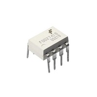
Manufacturer Part Number
HCPL2730
Description
High Speed Optocouplers DIP-8 DUAL PH DARL
Manufacturer
Fairchild Semiconductor
Datasheet
1.HCPL2730.pdf
(15 pages)
Specifications of HCPL2730
Input Type
DC
Isolation Voltage
2500 Vrms
Maximum Continuous Output Current
60 mA
Maximum Fall Time
35 us
Maximum Forward Diode Current
20 mA
Maximum Rise Time
20 us
Output Device
Darlington With Base
Configuration
2 Channel
Current Transfer Ratio
2500 %(Typ)
Maximum Baud Rate
100 KBps
Maximum Forward Diode Voltage
1.7 V
Maximum Reverse Diode Voltage
5 V
Maximum Input Diode Current
20 mA
Maximum Power Dissipation
100 mW
Maximum Operating Temperature
+ 85 C
Minimum Operating Temperature
- 40 C
Package / Case
PDIP Black
No. Of Channels
2
Optocoupler Output Type
Photodarlington
Input Current
1.6mA
Output Voltage
7V
Opto Case Style
DIP
No. Of Pins
8
Input Current Max
1.6mA
Rohs Compliant
Yes
Lead Free Status / RoHS Status
Lead free / RoHS Compliant
Other names
HCPL2730_NL
Available stocks
Company
Part Number
Manufacturer
Quantity
Price
Company:

Part Number:
HCPL2730
Manufacturer:
FSC
Quantity:
6 500
Company:
Part Number:
HCPL2730
Manufacturer:
AGILENT
Quantity:
20 000
Company:
Part Number:
HCPL2730500E
Manufacturer:
RFCN
Quantity:
4 825


©2005 Fairchild Semiconductor Corporation
6N138, 5N139, NCPL2730, HCPL2731 Rev. 1.0.5
Absolute Maximum Ratings
Stresses exceeding the absolute maximum ratings may damage the device. The device may not function or be
operable above the recommended operating conditions and stressing the parts to these levels is not recommended.
In addition, extended exposure to stresses above the recommended operating conditions may affect device reliability.
The absolute maximum ratings are stress ratings only.
EMITTER
DETECTOR
Symbol
I
I
V
F
I
O
F
I
T
T
T
F
CC
(trans) Peak Transient Input Current - ( 1µs P.W., 300 pps)
V
V
P
P
OPR
(avg)
STG
SOL
(avg)
(pk)
ER
, V
O
R
D
O
Storage Temperature
Operating Temperature
Lead Solder Temperature (Wave solder only. See recommended reflow profile
graph for SMD mounting)
DC/Average Forward Input Current
Peak Forward Input Current (50% duty cycle, 1 ms P.W.)
Reverse Input Voltage
Input Power Dissipation
Average Output Current
Emitter-Base Reverse Voltage
Supply Voltage, Output Voltage
Output Power Dissipation
(T
A
= 25°C unless otherwise specified)
Parameter
2
6N139, HCPL2731
Each Channel
Each Channel
Each Channel
Each Channel
Each Channel
6N138 and 6N139
6N138, HCPL2730
Each Channel
260 for 10 sec
-55 to +125
-40 to +85
-0.5 to 18
-0.5 to 7
Value
100
1.0
0.5
20
40
35
60
5
www.fairchildsemi.com
Units
mW
mW
mA
mA
mA
°C
°C
°C
A
V
V
V
Related parts for HCPL2730
Image
Part Number
Description
Manufacturer
Datasheet
Request
R

Part Number:
Description:
Fairchild Semiconductor [IGBT MODULE]
Manufacturer:
Fairchild Semiconductor
Datasheet:

Part Number:
Description:
Discrete Semiconductor Modules
Manufacturer:
Fairchild Semiconductor
Part Number:
Description:
Discrete Semiconductor Modules
Manufacturer:
Fairchild Semiconductor
Part Number:
Description:
This N-Channel MOSFET is produced using Fairchild Semiconductor’s advanced Power Trench® process
Manufacturer:
Fairchild Semiconductor
Datasheet:
Part Number:
Description:
This N-Channel MOSFET is produced using Fairchild Semiconductor’s advanced Power Trench® process
Manufacturer:
Fairchild Semiconductor
Datasheet:
Part Number:
Description:
This N-Channel MOSFET is produced using Fairchild Semiconductor’s advanced PowerTrench® process
Manufacturer:
Fairchild Semiconductor
Datasheet:
Part Number:
Description:
This N-Channel MOSFET is produced using Fairchild Semiconductor’s advanced PowerTrench® process
Manufacturer:
Fairchild Semiconductor
Datasheet:
Part Number:
Description:
This N-Channel MOSFET is produced using Fairchild Semiconductor’s advanced Power Trench® process
Manufacturer:
Fairchild Semiconductor
Datasheet:
Part Number:
Description:
This N-Channel logic Level MOSFETs are produced using Fairchild Semiconductor‘s advanced Power Trench® process that has been special tailored to minimize the on-state resistance and yet maintain superior switching performance
Manufacturer:
Fairchild Semiconductor
Datasheet:
Part Number:
Description:
This N-Channel MOSFET is produced using Fairchild Semiconductor’s advanced Power Trench® process
Manufacturer:
Fairchild Semiconductor
Datasheet:
Part Number:
Description:
This N-Channel SyncFET™ is produced using Fairchild Semiconductor’s advanced PowerTrench® process
Manufacturer:
Fairchild Semiconductor
Datasheet:
Part Number:
Description:
This N-Channel SyncFET™ is produced using Fairchild Semiconductor’s advanced PowerTrench® process
Manufacturer:
Fairchild Semiconductor
Datasheet:
Part Number:
Description:
This N-Channel SyncFET™ is produced using Fairchild Semiconductor’s advanced PowerTrench® process
Manufacturer:
Fairchild Semiconductor
Datasheet:
Part Number:
Description:
This N-Channel logic Level MOSFETs are produced using Fairchild Semiconductor‘s advanced Power Trench® process that has been special tailored to minimize the on-state resistance and yet maintain superior switching performance
Manufacturer:
Fairchild Semiconductor
Datasheet:
Part Number:
Description:
This N-Channel MOSFET is produced using Fairchild Semiconductor’s advanced Power Trench® process that has been especially tailored to minimize the on-state resistance and yet maintain superior switching performance
Manufacturer:
Fairchild Semiconductor
Datasheet: