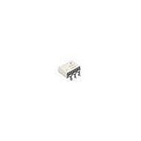
H11N1SVM Fairchild Semiconductor, H11N1SVM Datasheet - Page 2

H11N1SVM
Manufacturer Part Number
H11N1SVM
Description
High Speed Optocouplers Optocoupler LC Schmitt Trigger
Manufacturer
Fairchild Semiconductor
Datasheet
1.H11N1-M.pdf
(10 pages)
Specifications of H11N1SVM
Isolation Voltage
7.5 kV
Maximum Fall Time
12 us
Maximum Forward Diode Current
30 mA
Output Device
Logic Gate Photo IC
Configuration
1 Channel
Maximum Baud Rate
5 MBps
Maximum Forward Diode Voltage
2 V
Maximum Reverse Diode Voltage
6 V
Maximum Power Dissipation
250 mW
Maximum Operating Temperature
+ 85 C
Minimum Operating Temperature
- 40 C
Package / Case
PDIP W SMD
Lead Free Status / RoHS Status
Lead free / RoHS Compliant
Other names
H11N1SVM_NL
©2005 Fairchild Semiconductor Corporation
H11N1M, H11N2M, H11N3M Rev. 1.0.2
Absolute Maximum Ratings
Stresses exceeding the absolute maximum ratings may damage the device. The device may not function or be
operable above the recommended operating conditions and stressing the parts to these levels is not recommended.
In addition, extended exposure to stresses above the recommended operating conditions may affect device reliability.
The absolute maximum ratings are stress ratings only.
TOTAL DEVICE
EMITTER
DETECTOR
Symbol
I
T
T
T
F
V
P
V
P
P
V
OPR
STG
SOL
(pk)
I
I
CC
O
F
O
D
R
D
D
Storage Temperature
Operating Temperature
Lead Solder Temperature
Total Device Power Dissipation @ 25°C
Continuous Forward Current
Reverse Voltage
Forward Current – Peak (1µs pulse, 300 pps)
LED Power Dissipation 25°C Ambient
Detector Power Dissipation @ 25°C
V
V
I
4
45
65
Output Current
Derate Above 25°C
Derate Linearly From 25°C
Derate Linearly from 25°C
Allowed Range
Allowed Range
(T
A
Parameters
= 25°C unless otherwise specified.)
2
260 for 10 sec
-40 to +150
-40 to +85
0 to 16
0 to 16
Value
2.94
1.41
1.76
250
120
150
1.0
30
50
6
www.fairchildsemi.com
mW/°C
mW/°C
mW/°C
Units
mW
mW
mW
mA
mA
°C
°C
°C
V
A
V
V


