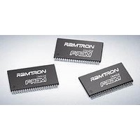
FM22L16-55-TG Ramtron, FM22L16-55-TG Datasheet - Page 4

FM22L16-55-TG
Manufacturer Part Number
FM22L16-55-TG
Description
F-RAM 4M (256Kx16) 55ns
Manufacturer
Ramtron
Datasheet
1.FM22L16-55-TG.pdf
(15 pages)
Specifications of FM22L16-55-TG
Organization
256 Kbit x 16
Access Time
55 ns
Operating Supply Voltage
2.7 V to 3.6 V
Operating Temperature Range
- 40 C to + 85 C
Mounting Style
SMD/SMT
Memory Size
4 Mbit
Interface
Parallel
Package / Case
TSOP-44
Lead Free Status / RoHS Status
Lead free / RoHS Compliant
Available stocks
Company
Part Number
Manufacturer
Quantity
Price
Company:
Part Number:
FM22L16-55-TG
Manufacturer:
RAM
Quantity:
15
Part Number:
FM22L16-55-TG
Manufacturer:
RAMTRON
Quantity:
20 000
Part Number:
FM22L16-55-TGKJ
Manufacturer:
CYPRESS/赛普拉斯
Quantity:
20 000
Company:
Part Number:
FM22L16-55-TGTR
Manufacturer:
CYPRESS
Quantity:
15 000
Overview
The FM21L16 is a wordwide F-RAM memory
logically organized as 131,072 x 16 and accessed
using an industry standard parallel interface. All data
written to the part is immediately nonvolatile with no
delay. The device offers page mode operation which
provides higher speed access to addresses within a
page (row). An access to a different page requires that
either /CE transitions low or the upper address
A(16:2) changes.
Memory Operation
Users access 131,072 memory locations, each with 16
data bits through a parallel interface. The F-RAM
array is organized as 8 blocks each having 4096 rows.
Each row has 4 column locations, which allows fast
access in page mode operation. Once an initial
address has been latched by the falling edge of /CE,
subsequent column locations may be accessed
without the need to toggle /CE.
deasserted high, a precharge operation begins. Writes
occur immediately at the end of the access with no
delay. The /WE pin must be toggled for each write
operation. The write data is stored in the nonvolatile
memory array immediately, which is a feature unique
to F-RAM called NoDelay
Read Operation
A read operation begins on the falling edge of /CE.
The falling edge of /CE causes the address to be
latched and starts a memory read cycle if /WE is high.
Data becomes available on the bus after the access
time has been satisfied. Once the address has been
latched and the access completed, a new access to a
random location (different row) may begin while /CE
is still low. The minimum cycle time for random
addresses is t
FM21L16’s /CE-initiated access time is faster than
the address cycle time.
The FM21L16 will drive the data bus when /OE and
at least one of the byte enables (/UB, /LB) is asserted
low. The upper data byte is driven when /UB is low,
and the lower data byte is driven when /LB is low. If
/OE is asserted after the memory access time has been
satisfied, the data bus will be driven with valid data.
If /OE is asserted prior to completion of the memory
access, the data bus will not be driven until valid data
is available. This feature minimizes supply current in
the system by eliminating transients caused by invalid
data being driven onto the bus. When /OE is
deasserted high, the data bus will remain in a high-Z
state.
Write Operation
Writes occur in the FM21L16 in the same time
interval as reads. The FM21L16 supports both /CE-
Rev. 2.0
Apr. 2011
RC
. Note that unlike SRAMs, the
TM
writes.
When /CE is
and /WE-controlled write cycles. In both cases, the
address A(16:2) is latched on the falling edge of /CE.
In a /CE-controlled write, the /WE signal is asserted
prior to beginning the memory cycle. That is, /WE is
low when /CE falls. In this case, the device begins the
memory cycle as a write. The FM21L16 will not
drive the data bus regardless of the state of /OE as
long as /WE is low. Input data must be valid when
/CE is deasserted high. In a /WE-controlled write, the
memory cycle begins on the falling edge of /CE. The
/WE signal falls some time later. Therefore, the
memory cycle begins as a read. The data bus will be
driven if /OE is low, however it will hi-Z once /WE is
asserted low. The /CE- and /WE-controlled write
timing
Specifications section.
Write access to the array begins on the falling edge of
/WE after the memory cycle is initiated. The write
access terminates on the rising edge of /WE or /CE,
whichever comes first. A valid write operation
requires the user to meet the access time specification
prior to deasserting /WE or /CE. Data setup time
indicates the interval during which data cannot
change prior to the end of the write access (rising
edge of /WE or /CE).
Unlike other truly nonvolatile memory technologies,
there is no write delay with F-RAM. Since the read
and write access times of the underlying memory are
the same, the user experiences no delay through the
bus. The entire memory operation occurs in a single
bus cycle. Data polling, a technique used with
EEPROMs to determine if a write is complete, is
unnecessary.
Page Mode Operation
The F-RAM array is organized as 8 blocks each
having 4096 rows. Each row has 4 column address
locations. Address inputs A(1:0) define the column
address to be accessed. An access can start on any
column address, and other column locations may be
accessed without the need to toggle the /CE pin. For
fast access reads, once the first data byte is driven
onto the bus, the column address inputs A(1:0) may
be changed to a new value. A new data byte is then
driven to the DQ pins no later than t
than half the initial read access time. For fast access
writes, the first write pulse defines the first write
access. While /CE is low, a subsequent write pulse
along with a new column address provides a page
mode write access.
cases
are
FM21L16 - 128Kx16 FRAM
shown
in
AAP
the
, which is less
Page 4 of 15
Electrical


