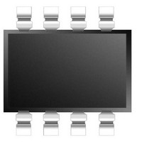
FAN7930BMX Fairchild Semiconductor, FAN7930BMX Datasheet - Page 12

FAN7930BMX
Manufacturer Part Number
FAN7930BMX
Description
Power Factor Correction ICs Critical Conduction Mode PFC Controller
Manufacturer
Fairchild Semiconductor
Datasheet
1.FAN7930BMX.pdf
(22 pages)
Specifications of FAN7930BMX
Switching Frequency
300 KHz
Maximum Operating Temperature
+ 125 C
Mounting Style
SMD/SMT
Minimum Operating Temperature
- 40 C
Package / Case
SOP-8
Lead Free Status / RoHS Status
Lead free / RoHS Compliant
Available stocks
Company
Part Number
Manufacturer
Quantity
Price
Company:
Part Number:
FAN7930BMX
Manufacturer:
FAIRCHILD
Quantity:
4 000
Part Number:
FAN7930BMX
Manufacturer:
FAIRCHILD/ن»™ç«¥
Quantity:
20 000
Part Number:
FAN7930BMX-G
Manufacturer:
FAIRCHILD/ن»™ç«¥
Quantity:
20 000
Company:
Part Number:
FAN7930BMX_G
Manufacturer:
FAIRCHILD
Quantity:
7 229
© 2010 Fairchild Semiconductor Corporation
FAN7930B • Rev. 1.0.2
Since the two OVP conditions are quite different,
protection recovering mode is different. Once the first
OVP triggers, switching stops immediately and recovers
switching when the output voltage is decreased with a
hysteresis. When the second OVP triggers, switching
can be recovered only when the V
below V
V
OVP is not used, the OVP pin must be connected to the
INV pin or to the ground.
4. Control Range Compensation: On time is controlled
by the output voltage compensator with FAN7930B. Due
to this when input voltage is high and load is light,
control range become narrow compared when input
voltage is low. That control range decrease is anti-
proportional to the double square of the input voltage.
Thus at high line unwanted burst operation easily
happens at light load and audible noise may be
generated from the boost inductor or inductor at input
filter. Different from the other converters, burst operation
in PFC block is not needed because PFC block itself is
normally disabled during standby mode. To improve this
kind of unwanted burst operation at light load, internal
control range compensation function is implemented
and approximately shows no burst operation until 5%
load at high line.
5. Zero-Current Detection: Zero-current detection
(ZCD) generates the turn-on signal of the MOSFET
when the boost inductor current reaches zero using an
auxiliary winding coupled with the inductor. When the
power switch turns on, negative voltage is induced at the
auxiliary winding due to the opposite winding direction
(see Equation 1) and positive voltage is induced (see
Equation 2) when the power switch turns off.
V
V
OVP
AUX
AUX
Figure 25.
should be lower than hysteresis. If the second
=
=
STOP
−
T
T
AUX
T
IND
T
AUX
IND
and builds up higher than V
⋅
(
⋅
V
V
PFCOUT
AC
Comparison of 1
Recovering Mode
−
V
AC
)
CC
st
supply voltage falls
and 2
START
nd
again and
OVP
(1)
(2)
12
where, V
T
respectively, V
V
Because auxiliary winding voltage can swing from
negative voltage to positive voltage, the internal block in
ZCD pin has both positive and negative voltage
clamping circuits. When the auxiliary voltage is
negative, internal circuit clamps the negative voltage at
the ZCD pin around 0.65V by sourcing current to the
serial resistor between the ZCD pin and the auxiliary
winding. When the auxiliary voltage is higher than 6.5V,
current is sinked through a resistor from the auxiliary
winding to the ZCD pin.
To check the boost inductor current zero instance,
auxiliary winding voltage is used. When boost inductor
current becomes zero, there is a resonance between
boost inductor and all capacitors at MOSFET drain pin,
including C
the D-S pin to reduce the voltage rising and falling slope
of the MOSFET; a parasitic capacitor at inductor; and so
on to improve performance. Resonated voltage is
reflected to the auxiliary winding and can be used as
detecting zero current of boost inductor and valley
position of MOSFET voltage stress. For valley detection,
a minor delay by the resistor and capacitor is needed. A
capacitor increases the noise immunity at the ZCD pin.
If ZCD voltage is higher than 1.5V, an internal ZCD
comparator output becomes HIGH and LOW when the
ZCD goes below 1.4V. At the falling edge of comparator
output, internal logic turns on the MOSFET.
AUX
OUT_PFC
are boost inductor turns and auxiliary winding turns
Figure 27. Auxiliary Voltage Depends
is output voltage from the PFC converter.
AUX
OSS
Figure 26.
is the auxiliary winding voltage, T
AC
of the MOSFET; an external capacitor at
on MOSFET Switching
is input voltage for PFC converter and
Circuit Near ZCD
www.fairchildsemi.com
IND
and


