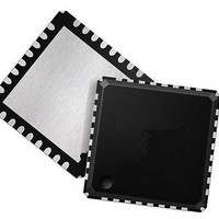
ispPAC-POWR607-01SN32I Lattice, ispPAC-POWR607-01SN32I Datasheet - Page 10

ispPAC-POWR607-01SN32I
Manufacturer Part Number
ispPAC-POWR607-01SN32I
Description
Supervisory Circuits Prec Prog Pwr Supply Seq Mon IND
Manufacturer
Lattice
Type
Power Supply Sequencer and Monitorr
Series
ispPAC®r
Datasheet
1.ISPPAC-POWR607-01SN32I.pdf
(28 pages)
Specifications of ispPAC-POWR607-01SN32I
Internal Hysteresis
Yes
Minimum Operating Temperature
- 40 C
Output Type
Open Collector / Drain
Power Fail Detection
Yes
Number Of Voltages Monitored
6
Monitored Voltage
Adj V
Undervoltage Threshold
Adj
Overvoltage Threshold
Adj
Manual Reset
Resettable
Watchdog
Yes
Power-up Reset Delay (typ)
100 us
Supply Voltage (max)
3.96 V
Supply Voltage (min)
2.64 V
Supply Current (typ)
3.5 mA
Mounting Style
SMD/SMT
Maximum Operating Temperature
+ 85 C
Package / Case
QFN-32
Applications
General Purpose
Voltage - Input
-0.3 V ~ 5.9 V
Voltage - Supply
2.64 V ~ 3.96 V
Current - Supply
3.5mA
Operating Temperature
-40°C ~ 85°C
Mounting Type
Surface Mount
Lead Free Status / RoHS Status
Lead free / RoHS Compliant
Available stocks
Company
Part Number
Manufacturer
Quantity
Price
Company:
Part Number:
ISPPAC-POWR607-01SN32I
Manufacturer:
LATTICE
Quantity:
284
Part Number:
ISPPAC-POWR607-01SN32I
Manufacturer:
LATTICE
Quantity:
20 000
Lattice Semiconductor
Figure 4-6. Verify Timing Diagram
Figure 4-7. Discharge Timing Diagram
Theory of Operation
Analog Monitor Inputs
The ispPAC-POWR607 provides six independently programmable voltage monitor input circuits as shown in
Figure 4-8. One programmable trip-point comparator is connected to each analog monitoring input. Each compara-
tor reference has 192 programmable trip points over the range of 0.667V to 5.811V. Additionally, a 75mV ‘zero-
detect’ threshold is selectable which allows the voltage monitors to determine if a monitored signal has dropped to
ground level. This feature is especially useful for determining if a power supply’s output has decayed to a substan-
tially inactive condition after it has been switched off.
Figure 4-8. ispPAC-POWR607 Voltage Monitors
Figure 4-8 shows the functional block diagram of one of the six voltage monitor inputs - ‘x’ (where x = 1...6). Each
voltage monitor can be divided into two sections: Analog Input, and Filtering.
The voltage input is monitored by a programmable trip-point comparator. Table 4-1 and Table 4-2 show all trip
points and ranges to which any comparator’s threshold can be set.
State
TCK
TMS
State
TCK
TMS
VIH
VIH
VIL
VIL
VIH
VIH
VIL
VIL
Update-IR
Update-IR
t
SU1
t
SU1
VMONx
t
CKH
t
H
Run-Test/Idle (Erase or Program)
t
CKH
t
SU1
t
t
H
CKL
t
SU1
t
CKL
Run-Test/Idle (Program)
t
H
Analog
ispPAC-POWR607
Input
Trip Point
t
H
t
PWP
t
SU1
t
PWV
t
Select-DR Scan
CKH
t
SU1
t
H
4-10
Select-DR Scan
t
CKH
t
H
Glitch
Filter
t
SU1
t
HVDIS
Signal
Logic
(Actual)
ispPAC-POWR607 Data Sheet
t
CKH
t
H
t
t
Run-Test/Idle (Verify)
SU1
SU1
t
CKL
Array
PLD
t
CKH
Specified by the Data Sheet
t
CKH
t
H
Update-IR
t
H
t
PWV
t
SU1
t
CKL
t
Actual
SU1
t
PWV
t
CKH
t
H
t
CKH
t
H


