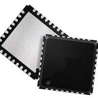
ispPAC-POWR607-01SN32I Lattice, ispPAC-POWR607-01SN32I Datasheet - Page 2

ispPAC-POWR607-01SN32I
Manufacturer Part Number
ispPAC-POWR607-01SN32I
Description
Supervisory Circuits Prec Prog Pwr Supply Seq Mon IND
Manufacturer
Lattice
Type
Power Supply Sequencer and Monitorr
Series
ispPAC®r
Datasheet
1.ISPPAC-POWR607-01SN32I.pdf
(28 pages)
Specifications of ispPAC-POWR607-01SN32I
Internal Hysteresis
Yes
Minimum Operating Temperature
- 40 C
Output Type
Open Collector / Drain
Power Fail Detection
Yes
Number Of Voltages Monitored
6
Monitored Voltage
Adj V
Undervoltage Threshold
Adj
Overvoltage Threshold
Adj
Manual Reset
Resettable
Watchdog
Yes
Power-up Reset Delay (typ)
100 us
Supply Voltage (max)
3.96 V
Supply Voltage (min)
2.64 V
Supply Current (typ)
3.5 mA
Mounting Style
SMD/SMT
Maximum Operating Temperature
+ 85 C
Package / Case
QFN-32
Applications
General Purpose
Voltage - Input
-0.3 V ~ 5.9 V
Voltage - Supply
2.64 V ~ 3.96 V
Current - Supply
3.5mA
Operating Temperature
-40°C ~ 85°C
Mounting Type
Surface Mount
Lead Free Status / RoHS Status
Lead free / RoHS Compliant
Available stocks
Company
Part Number
Manufacturer
Quantity
Price
Company:
Part Number:
ISPPAC-POWR607-01SN32I
Manufacturer:
LATTICE
Quantity:
284
Part Number:
ISPPAC-POWR607-01SN32I
Manufacturer:
LATTICE
Quantity:
20 000
Pin Descriptions
Lattice Semiconductor
and digital inputs used as inputs to the CPLD array. The digital output pins providing the external control signals are
driven by the CPLD. Four independently programmable timers also interface with the CPLD and can create delays
and time-outs ranging from 32µs to 2 seconds. The CPLD is programmed using LogiBuilder™, an easy-to-learn
language integrated into the PAC-Designer
the analog input channel comparators or the digital inputs.
Figure 4-1. ispPAC-POWR607 Block Diagram
Number
11, 12
30
31
27
26
23
22
20
29
IN1_PWRDN
IN_OUT3
IN_OUT4
IN_OUT5
IN_OUT6
IN_OUT7
HVOUT1
HVOUT2
Name
GND
IN1_PWRDN
Ground
Open Drain Output
FET Gate Driver
Open Drain Output
FET Gate Driver
Digital Input
Open Drain Output
Digital Input
Open Drain Output
Digital Input
Open Drain Output
Digital Input
Open Drain Output
Digital Input
Open Drain Output
Digital Input
VMON1
VMON2
VMON3
VMON4
VMON5
VMON6
IN2
Pin Type
9
9
9
9
9
®
Power Down
software. Control sequences are written to monitor the status of any of
4 Timers
Logic
2
2
2
2
2
2
2
Ground
0V to 10V
0V to 9V
0V to 10V
0V to 9V
0V to 5.5V
0V to 5.5V
0V to 5.5V
0V to 5.5V
0V to 5.5V
0V to 5.5V
4-2
VCC
Voltage Range
ispPAC-POWR607
JTAG Interface
16 Macrocells
28 Inputs
PLD
3
Ground
Open-Drain Output 1
High-voltage FET Gate Driver 1
Open-Drain Output 2
High-voltage FET Gate Driver 2
PLD Input 3
Open Drain Output 3
PLD Input 4
Open Drain Output 4
PLD Input 5
Open Drain Output 5
PLD Input 6
Open Drain Output 6
PLD Input 7
Open Drain Output 7
PLD Logic Input 1.
should be pulled down with a 10k Ω resistor.
ispPAC-POWR607 Data Sheet
HVOUT1
HVOUT2
IN_OUT3
IN_OUT4
IN_OUT5
IN_OUT6
IN_OUT7
1
Description
4, 5
When not used, this pin


