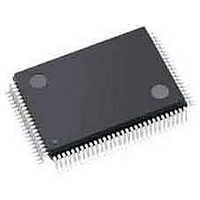
APA150-TQG100 Actel, APA150-TQG100 Datasheet - Page 174

APA150-TQG100
Manufacturer Part Number
APA150-TQG100
Description
FPGA - Field Programmable Gate Array 150K System Gates
Manufacturer
Actel
Datasheet
1.APA075-FGG144.pdf
(178 pages)
Specifications of APA150-TQG100
Processor Series
APA150
Core
IP Core
Maximum Operating Frequency
150 MHz
Number Of Programmable I/os
242
Data Ram Size
36864
Supply Voltage (max)
2.7 V
Maximum Operating Temperature
+ 70 C
Minimum Operating Temperature
0 C
Development Tools By Supplier
APA-Eval-Kit, APA-Eval-BRD1, Silicon-Explorer II, Silicon-Sculptor 3, SI-EX-TCA, Flashpro 4, Flashpro 3, Flashpro Lite
Mounting Style
SMD/SMT
Supply Voltage (min)
2.3 V
Number Of Gates
150 K
Package / Case
TQFP-100
Lead Free Status / RoHS Status
Lead free / RoHS Compliant
Available stocks
Company
Part Number
Manufacturer
Quantity
Price
Company:
Part Number:
APA150-TQG100A
Manufacturer:
Microsemi SoC
Quantity:
10 000
Company:
Part Number:
APA150-TQG100I
Manufacturer:
LT
Quantity:
1 400
Company:
Part Number:
APA150-TQG100I
Manufacturer:
Microsemi SoC
Quantity:
10 000
4 -6
Previous version
v2.0
(continued)
Advance v0.7
Advance v0.6
ProASIC
PLUS
Flash Family FPGAs
The following pins have been changed in the
Pin Number
U4
U6
U7
V5
V6
The
The
The
"I/O Features" section
The
section,
Options" section
"PLL Block – Top-Level View and Detailed PLL Block Diagram" section
Figure 2-12 • Input Connectors to ProASICPLUS Clock Conditioning Circuitry
"Sample Implementations"
Minimization" section
Figure 2-13 • Using the PLL 33 MHz In, 133 MHz
for Clock Deskewing
The
The
Figure 2-23 • Tristate Buffer Delays
The
The
The
Applies to Military Temperature and MIL-STD-883B Temperature Only
The
The
The
The
The
The
The
The
The
The
Pin AK31 of FG1152 for the APA1000 changed to V
The
The
The
The
The
Table 2-1 • Clock Spines
Figure 2-11 • PLL Block – Top-Level View and Detailed PLL Block Diagram
The
The
Changes in current version (v5.9)
"ProASIC
"Array Coordinates" section
"Power-Up Sequencing" section
"PLL Electrical Specifications" section
"Design Environment" section
"Calculating Typical Power Dissipation" section
"DC Electrical Specifications (V
"DC Specifications (3.3 V PCI Operation)1" section
"Tristate Buffer Delays" section
"Output Buffer Delays" section
"Input Buffer Delays" section
"Global Input Buffer Delays" section
"Predicted Global Routing Delay" section
"Global Routing Skew" section
"Sample Macrocell Library Listing" section
"Pin Description" section
"Recommended Design Practice for VPN/VPP" section
"Features and Benefits" section
"ProASICPLUS Product Profile" section
"Ordering Information" section
"Plastic Device Resources"
"ProASIC
"Design Environment" section
"Package Thermal Characteristics" section
Table 2-24 • DC Electrical Specifications (V
"Timing Control and Characteristics" section
"Functional Description"
PLUS
PLUS
are new.
Architecture" section
Architecture" section
Function
I/O (GLMX1)
NPECL1
GL1
GL2
PPECL1 (I/P)
are new.
was updated.
are new.
was updated.
section,
was updated. GLMX is new.
was updated.
and
was updated.
DDP
was updated.
was updated.
section,
(the figure and table) have been updated.
(the figure and table) have been updated.
was updated.
was updated.
was updated.
were updated.
is new.
"Adjustable Clock Delay"
Table 2-2 • Array Coordinates
= 2.5 V ±0.2V)" section
was updated.
was updated.
was updated.
is new.
was updated.
v5.9
"Lock Signal"
"1152-Pin FBGA"
was updated.
Pin Number
U29
U31
V28
V29
V30
was updated.
was updated.
DDP
Outthrough and
was updated.
PP
was updated.
= 3.3 V ±0.3 V and V
.
was updated.
was updated.
section, and
was updated.
table:
section, and the
Figure 2-17 • Using the PLL
"Physical Implementation"
Function
NPECL2
I/O (GLMX2)
PPECL2 (I/P)
GL4
GL3
are new.
was updated.
was updated.
was updated.
"PLL Configuration
DD
was updated.
= 2.5 V ±0.2 V)
"Clock Skew
2-10
2-14
Page
3-69
2-11
2-12
2-13
2-18
2-25
2-42
2-28
2-34
2-38
2-40
2-42
2-44
2-46
2-48
2-50
2-50
2-51
2-73
2-74
3-69
2-11
2-25
2-27
1-2
2-5
2-7
2-6
1-2
2-4
to
to
ii
ii
i
i
2-13
2-16


