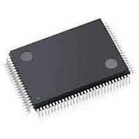
APA150-TQG100 Actel, APA150-TQG100 Datasheet - Page 22

APA150-TQG100
Manufacturer Part Number
APA150-TQG100
Description
FPGA - Field Programmable Gate Array 150K System Gates
Manufacturer
Actel
Datasheet
1.APA075-FGG144.pdf
(178 pages)
Specifications of APA150-TQG100
Processor Series
APA150
Core
IP Core
Maximum Operating Frequency
150 MHz
Number Of Programmable I/os
242
Data Ram Size
36864
Supply Voltage (max)
2.7 V
Maximum Operating Temperature
+ 70 C
Minimum Operating Temperature
0 C
Development Tools By Supplier
APA-Eval-Kit, APA-Eval-BRD1, Silicon-Explorer II, Silicon-Sculptor 3, SI-EX-TCA, Flashpro 4, Flashpro 3, Flashpro Lite
Mounting Style
SMD/SMT
Supply Voltage (min)
2.3 V
Number Of Gates
150 K
Package / Case
TQFP-100
Lead Free Status / RoHS Status
Lead free / RoHS Compliant
Available stocks
Company
Part Number
Manufacturer
Quantity
Price
Company:
Part Number:
APA150-TQG100A
Manufacturer:
Microsemi SoC
Quantity:
10 000
Company:
Part Number:
APA150-TQG100I
Manufacturer:
LT
Quantity:
1 400
Company:
Part Number:
APA150-TQG100I
Manufacturer:
Microsemi SoC
Quantity:
10 000
Note: When a signal from an I/O tile is connected to the core, it cannot be connected to the global MUX at the same time.
Figure 2-12 • Input Connectors to ProASIC
Table 2-7 •
2 -1 2
MUX
FBSEL
1
2
3
XDLYSEL
0
1
OBMUX
0
1
2
4
5
6
7
OAMUX
0
1
2
3
ProASIC
PLUS
Clock-Conditioning Circuitry MUX Settings
Flash Family FPGAs
Package Pins
Internal Feedback
Internal Feedback and Advance Clock Using FBDLY
External Feedback (EXTFB)
Feedback Unchanged
Deskew feedback by advancing clock by system delay
Primary bypass, no divider
Primary bypass, use divider
Delay Clock Using FBDLY
Phase Shift Clock by 0°
Reserved
Phase Shift Clock by +180°
Reserved
Secondary bypass, no divider
Secondary bypass, use divider
Delay Clock Using FBDLY
Phase Shift Clock by 0°
NPECL
PPECL
GLMX
GL
GL
Legend
PECL Pad Cell
Physical I/O
Physical Pin
DATA Signals to the Core
DATA Signals to the PLL Block
Std. Pad Cell
Std. Pad Cell
Std. Pad Cell
Buffers
Datapath
PLUS
GLA
GLB
Clock Conditioning Circuitry
CORE
v5.9
DATA Signals to the Global MUX
Control Signals to the Global MUX
Configuration Tile
Configuration Tile
–0.25 to –4 ns in 0.25 ns increments
Fixed delay of –2.95 ns
+0.25 to +4 ns in 0.25 ns increments
+0.25 to +4 ns in 0.25 ns increments
Global MUX
Comments
Global MUX B
OUT
External
Feedback
Global MUX A
OUT


