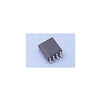
DG419BDQ-T1-E3 Vishay, DG419BDQ-T1-E3 Datasheet - Page 7

DG419BDQ-T1-E3
Manufacturer Part Number
DG419BDQ-T1-E3
Description
Analog Switch ICs Single SPDT 20/25V
Manufacturer
Vishay
Type
Analog Switchr
Specifications of DG419BDQ-T1-E3
Number Of Switches
Single
Switch Configuration
SPDT
On Resistance (max)
35 Ohms @ 12 V
On Time (max)
125 ns @ 12 V
Off Time (max)
66 ns @ 12 V
Off Isolation (typ)
- 82 dB
Supply Voltage (max)
25 V
Supply Current
0.000001 mA @ +/- 16.5 V
Maximum Power Dissipation
400 mW
Maximum Operating Temperature
+ 85 C
Mounting Style
SMD/SMT
Package / Case
MSOP
Minimum Operating Temperature
- 40 C
Off State Leakage Current (max)
12 nA
Propagation Delay Time
87 ns @ +/- 15V/119 ns @ 12V
Analog Switch Type
SPDT
No. Of Channels
1
On State Resistance Max
15ohm
Turn Off Time
38ns
Turn On Time
100ns
Supply Voltage Range
10.8V To 13.2V
Package
8MSOP
Maximum On Resistance
35@10.8V Ohm
Maximum Propagation Delay Bus To Bus
87@±15V|119@12V ns
Maximum High Level Output Current
30 mA
Number Of Channels Per Chip
1
Maximum Turn-off Time
80@±15V ns
Maximum Turn-on Time
125@12V ns
Switch Architecture
SPDT
Power Supply Type
Single|Dual
Lead Free Status / RoHS Status
Lead free / RoHS Compliant
Lead Free Status / RoHS Status
Lead free / RoHS Compliant, Lead free / RoHS Compliant
TEST CIRCUITS
V
Document Number: 70051
S10-1528-Rev. G, 19-Jul-10
O
V
V
± 10 V
V
V
S1
S2
S1
S2
is the steady state output with the switch on.
C
L
(includes fixture and stray capacitance)
S
S
IN
S
S
IN
GND
+ 5 V
GND
1
2
1
2
C
V
V
V
S
IN
GND
+ 5 V
L
L
O
L
V
(includes fixture and stray capacitance)
= V
L
+ 5 V
V
S
O
= V
S
+ 15 V
- 15 V
V+
V-
R
+ 15 V
- 15 V
- 15 V
L
D
V+
V-
R
V+
V-
+ r
L
DS(on)
R
D
D
+ 15 V
L
R
+ r
L
DS(on)
C
R
300
L
L
(includes fixture and stray capacitance)
R
300
R
300
L
L
Figure 2. Switching Time (DG417, DG418)
Figure 3. Break-Before-Make (DG419)
Figure 4. Transition Time (DG419)
C
35 pF
L
C
35 pF
C
35 pF
L
L
V
O
V
V
O
O
Note:
Logic
Input
Switch
Output
Logic
Input
Switch
Output
V
Logic
Input
Switch
Input
Switch
Output
S1
= V
Logic input waveform is inverted for switches that have the
opposite logic sense.
S2
V
V
V
V
3 V
0 V
3 V
0 V
0 V
S1
S2
O
01
3 V
0 V
0 V
V
S
DG417, DG418, DG419
50 %
90 %
t
TRANS
t
V
D
V
t
ON
02
O
50 %
90 %
10 %
Vishay Siliconix
t
TRANS
90 %
www.vishay.com
t
t
r
f
< 20 ns
< 20 ns
t
t
r
f
t
D
< 20 ns
< 20 ns
t
t
r
f
t
< 20 ns
< 20 ns
OFF
7


