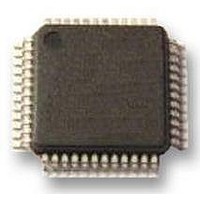
MC56F8256VLF Freescale Semiconductor, MC56F8256VLF Datasheet - Page 21

MC56F8256VLF
Manufacturer Part Number
MC56F8256VLF
Description
DSC 64K FLASH 60MHZ 48-LQFP
Manufacturer
Freescale Semiconductor
Series
56F8xxxr
Datasheets
1.TWR-56F8257.pdf
(88 pages)
2.MC56F8245VLD.pdf
(14 pages)
3.MC56F8245VLD.pdf
(2 pages)
4.MC56F8245VLD.pdf
(629 pages)
Specifications of MC56F8256VLF
Core Processor
56800E
Core Size
16-Bit
Speed
60MHz
Connectivity
CAN, I²C, LIN, SCI, SPI
Peripherals
LVD, POR, PWM, WDT
Number Of I /o
39
Program Memory Size
64KB (32K x 16)
Program Memory Type
FLASH
Ram Size
4K x 16
Voltage - Supply (vcc/vdd)
3 V ~ 3.6 V
Data Converters
A/D 10x12b, D/A 1x12b
Oscillator Type
Internal
Operating Temperature
-40°C ~ 105°C
Package / Case
48-LQFP
Product
DSCs
Processor Series
56800E
Core
56800E
Device Million Instructions Per Second
60 MIPs
Maximum Clock Frequency
60 MHz
Number Of Programmable I/os
39
Data Ram Size
8 KB
Operating Supply Voltage
3.3 V
Maximum Operating Temperature
+ 105 C
Mounting Style
SMD/SMT
Minimum Operating Temperature
- 40 C
On-chip Adc
12 bit, 5 Channel
Lead Free Status / RoHS Status
Lead free / RoHS Compliant
Eeprom Size
-
Lead Free Status / Rohs Status
Details
Available stocks
Company
Part Number
Manufacturer
Quantity
Price
Company:
Part Number:
MC56F8256VLF
Manufacturer:
AD
Quantity:
23
Company:
Part Number:
MC56F8256VLF
Manufacturer:
MOTOLOLA
Quantity:
413
Company:
Part Number:
MC56F8256VLF
Manufacturer:
Freescale Semiconductor
Quantity:
10 000
Part Number:
MC56F8256VLF
Manufacturer:
FREESCALE
Quantity:
20 000
Freescale Semiconductor
CMPB_M0)
CMPC_M0)
CMPB_P2)
CMPC_P2)
VREFHB&
VREFLB&
GPIOB0
GPIOB1
GPIOB2
GPIOB3
(ANB0&
(ANB1&
(ANB2&
(ANB3&
Signal
Name
LQFP
44
15
16
18
19
Table 5. MC56F825x/MC56F824x Signal and Package Information (continued)
LQFP
48
17
18
20
21
LQFP
64
24
25
27
28
MC56F825x/MC56F824x Digital Signal Controller, Rev. 3
Output
Output
Output
Output
Input/
Input/
Input/
Input/
Type
Input
Input
Input
Input
enabled
enabled
enabled
enabled
internal
internal
internal
internal
During
Reset
pullup
pullup
pullup
pullup
Input,
Input,
Input,
Input,
State
Port B GPIO — This GPIO pin can be individually programmed as
an input or output pin.
ANB0 and CMPB_P2 — Analog input to channel 0 of ADCB and
positive input 2 of analog comparator B.
When used as an analog input, the signal goes to ANB0 and
CMPB_P2.
After reset, the default state is GPIOB0.
Port B GPIO — This GPIO pin can be individually programmed as
an input or output pin.
ANB1 and CMPB_M0— Analog input to channel 1 of ADCB and
negative input 0 of analog comparator B.
When used as an analog input, the signal goes to ANB1 and
CMPB_M0.
After reset, the default state is GPIOB1.
Port B GPIO — This GPIO pin can be individually programmed as
an input or output pin.
ANB2 and VREFHB and CMPC_P2 — Analog input to channel 2 of
ADCB and analog references high of ADCB and positive input 2 of
analog comparator C.
When used as an analog input, the signal goes to ANB2 and
VREFHB and CMPC_P2. ADC control register configures this input
as ANB2 or VREFHB.
After reset, the default state is GPIOB2.
Port B GPIO — This GPIO pin can be individually programmed as
an input or output pin.
ANB3 and VREFLB and CMPC_M0 — Analog input to channel 3 of
ADCB and analog references low of ADCB and negative input 0 of
analog comparator C.
When used as an analog input, the signal goes to ANB3 and
VREFLB and MPC_M0. ADC control register configures this input
as ANB3 or VREFLB.
After reset, the default state is GPIOB3.
Signal Description
Signal/Connection Descriptions
21


