MC56F8256VLF Freescale Semiconductor, MC56F8256VLF Datasheet - Page 46
MC56F8256VLF
Manufacturer Part Number
MC56F8256VLF
Description
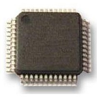
DSC 64K FLASH 60MHZ 48-LQFP
Manufacturer
Freescale Semiconductor
Series
56F8xxxr
Datasheets
1.TWR-56F8257.pdf
(88 pages)
2.MC56F8245VLD.pdf
(14 pages)
3.MC56F8245VLD.pdf
(2 pages)
4.MC56F8245VLD.pdf
(629 pages)
Specifications of MC56F8256VLF
Core Processor
56800E
Core Size
16-Bit
Speed
60MHz
Connectivity
CAN, I²C, LIN, SCI, SPI
Peripherals
LVD, POR, PWM, WDT
Number Of I /o
39
Program Memory Size
64KB (32K x 16)
Program Memory Type
FLASH
Ram Size
4K x 16
Voltage - Supply (vcc/vdd)
3 V ~ 3.6 V
Data Converters
A/D 10x12b, D/A 1x12b
Oscillator Type
Internal
Operating Temperature
-40°C ~ 105°C
Package / Case
48-LQFP
Product
DSCs
Processor Series
56800E
Core
56800E
Device Million Instructions Per Second
60 MIPs
Maximum Clock Frequency
60 MHz
Number Of Programmable I/os
39
Data Ram Size
8 KB
Operating Supply Voltage
3.3 V
Maximum Operating Temperature
+ 105 C
Mounting Style
SMD/SMT
Minimum Operating Temperature
- 40 C
On-chip Adc
12 bit, 5 Channel
Lead Free Status / RoHS Status
Lead free / RoHS Compliant
Eeprom Size
-
Lead Free Status / Rohs Status
Details
Available stocks
Company
Part Number
Manufacturer
Quantity
Price
Company:

Part Number:
MC56F8256VLF
Manufacturer:
AD
Quantity:
23
Company:
Part Number:
MC56F8256VLF
Manufacturer:
MOTOLOLA
Quantity:
413
Company:
Part Number:
MC56F8256VLF
Manufacturer:
Freescale Semiconductor
Quantity:
10 000
Part Number:
MC56F8256VLF
Manufacturer:
FREESCALE
Quantity:
20 000


Security Features
State of PWM2_EXTB:
5.8
The 56800E family includes extensive integrated support for application software development and real-time debugging. Two
modules, the Enhanced On-Chip Emulation (EOnCE) module and the core test access port (TAP, commonly called the JTAG
port), work together to provide these capabilities. Both are accessed through a common 4-pin JTAG/EOnCE interface. These
modules allow you to insert the MC56F825x/MC56F824x into a target system while retaining debug control. This capability is
especially important for devices without an external bus, because it eliminates the need for a costly cable to bring out the
footprint of the chip, as is required by a traditional emulator system.
The 56800E’s EOnCE module is a Freescale-designed module for developing and debugging application software used with
the chip. This module allows non-intrusive interaction with the CPU and is accessible through the pins of the JTAG interface
or by software program control of the 56800E core. Among the many features of the EOnCE module is support, in real-time
program execution, for data communication between the controller and the host software development and debug systems.
Other features allow for hardware breakpoints, the monitoring and tracking of program execution, and the ability to examine
and modify the contents of registers, memory, and on-chip peripherals, all in a special debug environment. No user-accessible
resources must be sacrificed to perform debugging operations.
The 56800E’s JTAG port provides an interface for the EOnCE module to the JTAG pins. The Joint Test Action Group (JTAG)
boundary scan is an IEEE 1149.1 standard methodology enabling access to test features using a test access port (TAP). A JTAG
boundary scan consists of a TAP controller and boundary scan registers. Contact your Freescale sales representative or
authorized distributor for device-specific BSDL information.
6
The MC56F825x/MC56F824x offers security features intended to prevent unauthorized users from gaining access to and
reading the contents of the flash memory (FM) array. The MC56F825x/MC56F824x’s flash memory security consists of several
hardware interlocks.
After flash memory security is set, the application software can allow an authorized user to access on-chip memory by including
a user-defined software subroutine that reads and transfers the contents of internal memory via peripherals. This application
software can communicate over a serial port, for example, to validate the authenticity of the requested access and then to grant
it until the next device reset. The system designer must use discretion when deciding whether to support this type of “back door”
access technique.
6.1
After you have programmed flash with the application code, or as part of programming the flash with the application code, you
can secure the MC56F825x/MC56F824x by programming the values 1 and 0 into bits 1 and 0, respectively, of program memory
location 0x00_7FF7. The CodeWarrior IDE menu flash lock command can also accomplish this task. The nonvolatile security
46
•
•
•
If the ADC conversion result in SAMPLE1 is less than the value programmed into the low limit register 1,
PWM1_EXTB is driven high.
If the ADC conversion result in SAMPLE2 is greater than the value programmed into the high limit register 2,
PWM2_EXTB is driven low.
If the ADC conversion result in SAMPLE2 is less than the value programmed into the low limit register 2,
PWM2_EXTB is driven high.
Joint Test Action Group (JTAG)/Enhanced On-Chip Emulator
(EOnCE)
Security Features
Operation with Security Enabled
In normal operation, an external pullup on the TMS pin is highly recommend to place the
JTAG state machine in reset state (if this pin is not configured as GPIO).
MC56F825x/MC56F824x Digital Signal Controller, Rev. 3
NOTE
Freescale Semiconductor
Related parts for MC56F8256VLF
Image
Part Number
Description
Manufacturer
Datasheet
Request
R

Part Number:
Description:
Manufacturer:
Freescale Semiconductor, Inc
Datasheet:
Part Number:
Description:
Manufacturer:
Freescale Semiconductor, Inc
Datasheet:
Part Number:
Description:
Manufacturer:
Freescale Semiconductor, Inc
Datasheet:
Part Number:
Description:
Manufacturer:
Freescale Semiconductor, Inc
Datasheet:
Part Number:
Description:
Manufacturer:
Freescale Semiconductor, Inc
Datasheet:
Part Number:
Description:
Manufacturer:
Freescale Semiconductor, Inc
Datasheet:
Part Number:
Description:
Manufacturer:
Freescale Semiconductor, Inc
Datasheet:
Part Number:
Description:
Manufacturer:
Freescale Semiconductor, Inc
Datasheet:
Part Number:
Description:
Manufacturer:
Freescale Semiconductor, Inc
Datasheet:
Part Number:
Description:
Manufacturer:
Freescale Semiconductor, Inc
Datasheet:
Part Number:
Description:
Manufacturer:
Freescale Semiconductor, Inc
Datasheet:
Part Number:
Description:
Manufacturer:
Freescale Semiconductor, Inc
Datasheet:
Part Number:
Description:
Manufacturer:
Freescale Semiconductor, Inc
Datasheet:
Part Number:
Description:
Manufacturer:
Freescale Semiconductor, Inc
Datasheet:
Part Number:
Description:
Manufacturer:
Freescale Semiconductor, Inc
Datasheet: