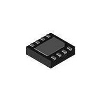
NCT1008DMN3R2G ON Semiconductor, NCT1008DMN3R2G Datasheet - Page 12

NCT1008DMN3R2G
Manufacturer Part Number
NCT1008DMN3R2G
Description
IC TEMP MONITOR 2CH DGTL 8-DFN
Manufacturer
ON Semiconductor
Datasheet
1.NCT1008CMT3R2G.pdf
(20 pages)
Specifications of NCT1008DMN3R2G
Function
Temp Monitoring System (Sensor)
Topology
ADC (Sigma Delta), Comparator, Multiplexer, Register Bank
Sensor Type
External & Internal
Sensing Temperature
0°C ~ 127°C, -64°C ~ 191°C
Output Type
I²C™/SMBus™
Output Alarm
Yes
Output Fan
Yes
Voltage - Supply
2.8 V ~ 3.6 V
Operating Temperature
-40°C ~ 125°C
Mounting Type
Surface Mount
Package / Case
8-VFDFN Exposed Pad
Full Temp Accuracy
+/- 1 C
Digital Output - Bus Interface
2 Wire, SMBus, I2C
Digital Output - Number Of Bits
8 bit
Supply Voltage (max)
3.6 V
Supply Voltage (min)
2.8 V
Description/function
Temperature Monitor with Series Resistance Cancellation
Supply Current
240 uA
Lead Free Status / RoHS Status
Lead free / RoHS Compliant
Available stocks
Company
Part Number
Manufacturer
Quantity
Price
Company:
Part Number:
NCT1008DMN3R2G
Manufacturer:
ON Semiconductor
Quantity:
2 350
1. Writing to Address 0x0F causes the NCT1008 to perform a single measurement. It is not a data register, and it does not matter what data
Serial Bus Interface
The NCT1008 is connected to this bus as a slave device,
under the control of a master device.
this is enabled, the SMBus/I
ms of no activity. However, this feature is not enabled by
default. Bit 7 of the consecutive alert register (Address =
0x22) should be set to enable it.
Addressing the Device
address, except for some devices that have extended 10−bit
addresses. When the master device sends a device address
over the bus, the slave device with that address responds.
The NCT1008 is available with one device address, 0x4C
(1001 100b). An NCT1008D is also available.
(1001 101b). This is to allow two NCT1008 devices on the
same bus, or if the default address conflicts with an existing
device on the SMBus/I
as follows:
Table 8. List of Registers
Read Address (Hex)
Control of the NCT1008 is carried out via the serial bus.
The NCT1008 has an SMBus/I
In general, every SMBus/I
The NCT1008D has an SMBus/I
is written to it.
Not Applicable
Not Applicable
1. The master initiates a data transfer by establishing
a start condition, defined as a high−to−low
transition on SDATA, the serial data line, while
FE
FF
00
01
02
03
04
05
06
07
08
10
12
13
14
19
20
21
22
11
2
C. The serial bus protocol operates
Write Address (Hex)
Not Applicable
Not Applicable
Not Applicable
Not Applicable
Not Applicable
Not Applicable
Not Applicable
2
0F (Note 1)
C times out after typically 25
2
C device has a 7−bit device
0C
0D
09
0A
0B
0E
12
13
14
19
20
21
22
11
2
C timeout feature. When
2
C address of 0x4D
Address Pointer
Local Temperature Value
External Temperature Value High Byte
Status
Configuration
Conversion Rate
Local Temperature High Limit
Local Temperature Low Limit
External Temperature High Limit High Byte
External Temperature Low Limit High Byte
One−Shot
External Temperature Value Low Byte
External Temperature Offset High Byte
External Temperature Offset Low Byte
External Temperature High Limit Low Byte
External Temperature Low Limit Low Byte
External THERM Limit
Local THERM Limit
THERM Hysteresis
Consecutive ALERT
Manufacturer ID
Die Revision Code
http://onsemi.com
12
Name
2. Data is sent over the serial bus in a sequence of
SCLK, the serial clock line, remains high. This
indicates that an address/data stream follows. All
slave peripherals connected to the serial bus
respond to the start condition and shift in the next
eight bits, consisting of a 7−bit address (MSB first)
plus an R/W bit, which determines the direction of
the data transfer, that is, whether data is written to,
or read from, the slave device. The peripheral
whose address corresponds to the transmitted
address responds by pulling the data line low
during the low period before the ninth clock pulse,
known as the acknowledge bit. All other devices
on the bus remain idle while the selected device
waits for data to be read from or written to it. If the
R/W bit is a 0, the master writes to the slave
device. If the R/W bit is a 1, the master reads from
the slave device.
nine clock pulses, eight bits of data followed by an
acknowledge bit from the slave device. Transitions
on the data line must occur during the low period
of the clock signal and remain stable during the
high period, since a low−to−high transition when
the clock is high can be interpreted as a stop
Undefined
0000 0000 (0x00)
0000 0000 (0x00)
Undefined
0000 0000 (0x00)
0000 1000 (0x08)
0101 0101 (0x55) (85°C)
0000 0000 (0x00) (0°C)
0101 0101 (0x55) (85°C)
0000 0000 (0x00) (0°C)
0000 0000
0000 0000
0000 0000
0000 0000
0000 0000
0110 1100 (0x6C) (108°C)
0101 0101 (0x55) (85°C)
0000 1010 (0x0A) (10°C)
0000 0001 (0x01)
0100 0001 (0x41)
0101 0111 (0x57)
Power−On Default


