AD650JP Analog Devices Inc, AD650JP Datasheet - Page 11
AD650JP
Manufacturer Part Number
AD650JP
Description
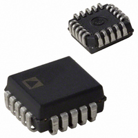
IC, V/F & F/V CONVERTER 1MHZ 0.1% LCC-20
Manufacturer
Analog Devices Inc
Type
Volt to Freq & Freq to Voltr
Datasheet
1.AD650KNZ.pdf
(20 pages)
Specifications of AD650JP
Full Scale Range
1MHz
Linearity %
0.005%
Supply Voltage Range
± 9V To ± 18V
Digital Ic Case Style
LCC
No. Of Pins
20
Frequency Max
1MHz
Termination Type
SMD
Mounting Type
Surface Mount
Rohs Status
RoHS non-compliant
Frequency - Max
1MHz
Full Scale
±150ppm/°C
Linearity
±0.1%
Package / Case
20-LCC (J-Lead)
Converter Function
VFC/FVC
Full Scale Frequency
1000
Power Supply Requirement
Dual
Single Supply Voltage (typ)
Not RequiredV
Single Supply Voltage (max)
Not RequiredV
Single Supply Voltage (min)
Not RequiredV
Dual Supply Voltage (min)
±9V
Dual Supply Voltage (max)
±18V
Operating Temperature (min)
0C
Operating Temperature (max)
70C
Operating Temperature Classification
Commercial
Package Type
PLCC
Filter Terminals
SMD
Rohs Compliant
No
Calibration Error Fs Typ
5%
Lead Free Status / RoHS Status
Contains lead / RoHS non-compliant
Lead Free Status / RoHS Status
Contains lead / RoHS non-compliant
Available stocks
Company
Part Number
Manufacturer
Quantity
Price

Company:
Part Number:
AD650JPZ
Manufacturer:
A-BRIGHT
Quantity:
30 000


0V TO 10V
V
IN
–15V
R3
–15V
–V
ADJUST
GAIN
IN
R3
R1
5kΩ
R1
–15V
Figure 12. Connection Diagram for V/F Conversion, Negative Input Voltage
14.3kΩ
0.1µF
C
OS
0.1µF
C
C
C
INT
OS
INT
51pF
Figure 13. Connection Diagram for F/V Conversion
0.1µF
3.6kΩ
1
2
3
4
5
6
7
1000pF
1
2
3
4
5
6
7
FREQ
Figure 14. 1 MHz V/F Connection Diagram
FREQ
–V
–V
S
OUT
S
1
2
3
4
5
6
7
SHOT
OUT
ONE
AMP
SHOT
OP
FREQ
ONE
Rev. D | Page 11 of 20
AMP
OP
–V
AD650
IN
OUT
S
OUT
AD650
IN
OUT
–V
SHOT
ONE
AMP
–V
S
OP
S1
1mA
S
S1
1mA
AD650
IN
OUT
–0.6V
–V
OFFSET
INPUT
COMP
–0.6V
TRIM
S
OFFSET
S1
INPUT
1mA
COMP
TRIM
–0.6V
14
13
12
11
10
9
8
OFFSET
INPUT
COMP
14
13
12
11
10
20kΩ
TRIM
1N914
9
8
250kΩ
20kΩ
DIGITAL
0.1µF
14
13
12
11
10
GND
9
8
500Ω
0.1µF
2kΩ
20kΩ
250kΩ
1µF
250kΩ
ANALOG
GND
0.1µF
1µF
510Ω
560pF
500Ω
V
+15V
OFFSET
ADJUST
OUT
R2
ANALOG
GND
DIGITAL
GND
ANALOG
GND PLANE
+V
+5V
F
0MHz TO 1MHz
+15V
F
+15V
OUT
OUT
F
+5V
LOGIC
IN
AD650
Related parts for AD650JP
Image
Part Number
Description
Manufacturer
Datasheet
Request
R

Part Number:
Description:
±1.7g Dual-Axis IMEMS Accelerometer Evaluation Board
Manufacturer:
Analog Devices Inc
Datasheet:

Part Number:
Description:
Inertial Sensor Evaluation System
Manufacturer:
Analog Devices Inc
Datasheet:
Part Number:
Description:
Manufacturer:
Analog Devices Inc
Datasheet:
Part Number:
Description:
Manufacturer:
Analog Devices Inc
Datasheet:
Part Number:
Description:
Manufacturer:
Analog Devices Inc
Datasheet:
Part Number:
Description:
Manufacturer:
Analog Devices Inc
Datasheet:
Part Number:
Description:
Manufacturer:
Analog Devices Inc
Datasheet:
Part Number:
Description:
Manufacturer:
Analog Devices Inc
Datasheet:
Part Number:
Description:
Manufacturer:
Analog Devices Inc
Datasheet:
Part Number:
Description:
Manufacturer:
Analog Devices Inc
Datasheet:
Part Number:
Description:
Manufacturer:
Analog Devices Inc
Datasheet:
Part Number:
Description:
Manufacturer:
Analog Devices Inc
Datasheet:
Part Number:
Description:
Manufacturer:
Analog Devices Inc
Datasheet: