AD650JP Analog Devices Inc, AD650JP Datasheet - Page 17
AD650JP
Manufacturer Part Number
AD650JP
Description
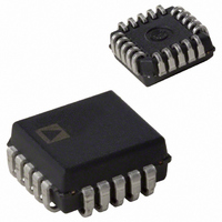
IC, V/F & F/V CONVERTER 1MHZ 0.1% LCC-20
Manufacturer
Analog Devices Inc
Type
Volt to Freq & Freq to Voltr
Datasheet
1.AD650KNZ.pdf
(20 pages)
Specifications of AD650JP
Full Scale Range
1MHz
Linearity %
0.005%
Supply Voltage Range
± 9V To ± 18V
Digital Ic Case Style
LCC
No. Of Pins
20
Frequency Max
1MHz
Termination Type
SMD
Mounting Type
Surface Mount
Rohs Status
RoHS non-compliant
Frequency - Max
1MHz
Full Scale
±150ppm/°C
Linearity
±0.1%
Package / Case
20-LCC (J-Lead)
Converter Function
VFC/FVC
Full Scale Frequency
1000
Power Supply Requirement
Dual
Single Supply Voltage (typ)
Not RequiredV
Single Supply Voltage (max)
Not RequiredV
Single Supply Voltage (min)
Not RequiredV
Dual Supply Voltage (min)
±9V
Dual Supply Voltage (max)
±18V
Operating Temperature (min)
0C
Operating Temperature (max)
70C
Operating Temperature Classification
Commercial
Package Type
PLCC
Filter Terminals
SMD
Rohs Compliant
No
Calibration Error Fs Typ
5%
Lead Free Status / RoHS Status
Contains lead / RoHS non-compliant
Lead Free Status / RoHS Status
Contains lead / RoHS non-compliant
Available stocks
Company
Part Number
Manufacturer
Quantity
Price

Company:
Part Number:
AD650JPZ
Manufacturer:
A-BRIGHT
Quantity:
30 000


PHASE-LOCKED LOOP F/V CONVERSION
Although the F/V conversion technique shown in Figure 13 is
quite accurate and uses only a few extra components, it is very
limited in terms of signal frequency response and carrier feed-
through. If the carrier (or input) frequency changes
instantaneously, then the output cannot change very rapidly due
to the integrator time constant formed by C
is possible to decrease the integrator time constant to provide
faster settling of the F-to-V output voltage, the carrier
feedthrough then becomes larger. For signal frequency response
in excess of 2 kHz, a phase-locked F/V conversion technique
such as the one shown in Figure 22 is recommended.
CONTROL
–5 VOLTS
INPUT
GND
–V
+V
S
S
CARRIER
CARRIER
AUTO ZERO
VFC NORMAL
INPUT
2
3
1
2
3
4
5
6
7
INPUT
1
4
AD7512
AD582
11
3
–V
10
D
FREQ
5
INT
D
S
CLOCK
CLOCK
OUT
12
2
2
1
1
1
PR
and R
1/2 7474
1/2 7474
PR
4
10
+V
14
13
12
11
10
6
9
9
8
2
VOLTAGE
1
S
D TYPE FLIP FLOP
AD650
1MHz FULL-SCALE
R
C
C
(UNIPOLAR INPUT)
INPUT
1
2
CLEAR
Figure 22. Phase-Locked Loop F/V Conversion
IN
OS
INT
0.1µF
8
7
CAP
CLEAR
13
1
IN
= 16.9k
16.9kΩ
OUTPUT
= 51pF
= 1000pF
. While it
Q
2
Q
1
2
1
10kΩ
Figure 21. Autozero Circuit
9
5
3
+V
3
2
Rev. D | Page 17 of 20
1000pF
1/4 7400
S
+IN
–IN
1kΩ
200kΩ
NAND
4
NULL
BIPOLAR
OFFSET
0.5mA
VOLTS INPUT
TO AD650
14
2
1
1000pF
OP
AMP
–15V
13
5
71.5kΩ
4
5
SD211
DMOSFET
In a phase-locked loop circuit, the oscillator is driven to a
frequency and phase equal to an input reference signal. In
applications such as a synthesizer, the oscillator output
frequency is first processed through a programmable “divide by
N” before being applied to the phase detector as feedback. Here
the oscillator frequency is forced to be equal to “N times” the
reference frequency. It is this frequency output that is the
desired output signal and not a voltage. In this case, the AD650
offers compact size and wide dynamic range.
XOR
–V
590kΩ
0.1µF
1mA
7486
1
S
–0.6 VOLT
–V
+15V
+V
9
COMPARATOR
12
S
COMPARATOR
INPUT
6
–15V
3.6kΩ
S
0.1µF
S
ANALOG
GND
GND
B
G
11
D
SHOT
51pF
ONE
51pF
C
FREQUENCY
AD509
OP AMP
6
15pF
VOLTAGE
140kΩ
OUTPUT
AD650
C
OUTPUT
OS
R
DIGITAL
F/V
GND
10
8
FREQUENCY
OUTPUT
500Ω
10µF
+
+5V
AD650
Related parts for AD650JP
Image
Part Number
Description
Manufacturer
Datasheet
Request
R

Part Number:
Description:
±1.7g Dual-Axis IMEMS Accelerometer Evaluation Board
Manufacturer:
Analog Devices Inc
Datasheet:

Part Number:
Description:
Inertial Sensor Evaluation System
Manufacturer:
Analog Devices Inc
Datasheet:
Part Number:
Description:
Manufacturer:
Analog Devices Inc
Datasheet:
Part Number:
Description:
Manufacturer:
Analog Devices Inc
Datasheet:
Part Number:
Description:
Manufacturer:
Analog Devices Inc
Datasheet:
Part Number:
Description:
Manufacturer:
Analog Devices Inc
Datasheet:
Part Number:
Description:
Manufacturer:
Analog Devices Inc
Datasheet:
Part Number:
Description:
Manufacturer:
Analog Devices Inc
Datasheet:
Part Number:
Description:
Manufacturer:
Analog Devices Inc
Datasheet:
Part Number:
Description:
Manufacturer:
Analog Devices Inc
Datasheet:
Part Number:
Description:
Manufacturer:
Analog Devices Inc
Datasheet:
Part Number:
Description:
Manufacturer:
Analog Devices Inc
Datasheet:
Part Number:
Description:
Manufacturer:
Analog Devices Inc
Datasheet: