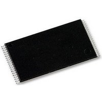
S29AL032D90TFI000 Spansion Inc., S29AL032D90TFI000 Datasheet - Page 35

S29AL032D90TFI000
Manufacturer Part Number
S29AL032D90TFI000
Description
Flash Memory IC
Manufacturer
Spansion Inc.
Specifications of S29AL032D90TFI000
Memory Size
32Mbit
Memory Configuration
4M X 8
Ic Interface Type
CFI, Parallel
Access Time
90ns
Supply Voltage Range
2.7 To 3.6 V
Memory Case Style
TSOP
No. Of Pins
40
Memory Type
Uniform Sector Flash
Interface Type
CFI
Rohs Compliant
Yes
Cell Type
NOR
Density
32Mb
Access Time (max)
90ns
Boot Type
Top
Address Bus
22/21Bit
Operating Supply Voltage (typ)
3/3.3V
Operating Temp Range
-40C to 85C
Package Type
TSOP
Sync/async
Asynchronous
Operating Temperature Classification
Industrial
Operating Supply Voltage (min)
2.7V
Operating Supply Voltage (max)
3.6V
Word Size
8/16Bit
Number Of Words
4M/2M
Supply Current
35mA
Mounting
Surface Mount
Pin Count
48
Lead Free Status / Rohs Status
Compliant
Available stocks
Company
Part Number
Manufacturer
Quantity
Price
11.4
11.5
11.6
January 19, 2007 S29AL032D_00_A9
Enter Secured Silicon Sector/Exit Secured Silicon Sector
Command Sequence
Word/Byte Program Command Sequence
Unlock Bypass Command Sequence
The Secured Silicon Sector region provides a secured data area containing a random, sixteen-byte electronic
serial number (ESN). The system can access the Secured Silicon Sector region by issuing the three-cycle
Enter Secured Silicon Sector command sequence. The device continues to access the Secured Silicon
Sector region until the system issues the four-cycle Exit Secured Silicon Sector command sequence. The Exit
Secured Silicon Sector command sequence returns the device to normal operation.
and
that the ACC function and unlock bypass modes are not available when the device enters the Secured Silicon
Sector. See also
Models 03, 04 may program the device by word or byte, depending on the state of the BYTE# pin. Model 00
may program the device by byte only. Programming is a four-bus-cycle operation. The program command
sequence is initiated by writing two unlock write cycles, followed by the program set-up command. The
program address and data are written next, which in turn initiate the Embedded Program algorithm. The
system is not required to provide further controls or timings. The device automatically generates the program
pulses and verifies the programmed cell margin.
requirements for the byte program command sequence.
When the Embedded Program algorithm is complete, the device then returns to reading array data and
addresses are no longer latched. The system can determine the status of the program operation by using
DQ7, DQ6, or RY/BY#. See
Any commands written to the device during the Embedded Program Algorithm are ignored. Note that a
hardware reset immediately terminates the programming operation. The Byte Program command sequence
should be reinitiated once the device has reset to reading array data, to ensure data integrity.
Programming is allowed in any sequence and across sector boundaries. A bit cannot be programmed from
a 0 back to a 1. Attempting to do so may halt the operation and set DQ5 to 1, or cause the Data# Polling
algorithm to indicate the operation was successful. However, a succeeding read will show that the data is still
0. Only erase operations can convert a 0 to a 1.
The unlock bypass feature allows the system to program bytes or words to the device faster than using the
standard program command sequence. The unlock bypass command sequence is initiated by first writing two
unlock cycles. This is followed by a third write cycle containing the unlock bypass command, 20h. The device
then enters the unlock bypass mode. A two-cycle unlock bypass program command sequence is all that is
required to program in this mode. The first cycle in this sequence contains the unlock bypass program
command, A0h; the second cycle contains the program address and data. Additional data is programmed in
the same manner. This mode dispenses with the initial two unlock cycles required in the standard program
command sequence, resulting in faster total programming time.
requirements for the command sequence.
During the unlock bypass mode, only the Unlock Bypass Program and Unlock Bypass Reset commands are
valid. To exit the unlock bypass mode, the system must issue the two-cycle unlock bypass reset command
sequence. The first cycle must contain the data 90h; the second cycle the data 00h. Addresses are don’t care
for both cycles. The device then returns to reading array data.
Figure 11.1 on page 34
Operations on page 52
Table 11.2 on page 38
Secured Silicon Sector Flash Memory Region on page 26
for parameters, and to
illustrates the algorithm for the program operation. See the
D a t a
show the addresses and data requirements for both command sequences. Note
Write Operation Status on page 40
S h e e t
S29AL032D
Figure 17.5 on page 53
Table 11.2 on page 38
Table 11.2 on page 38
for information on these status bits.
for timing diagrams.
shows the address and data
for further information.
Erase/Program
Table 11.1 on page 37
shows the
33


