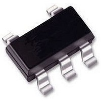
74HC1G66GW NXP Semiconductors, 74HC1G66GW Datasheet - Page 10

74HC1G66GW
Manufacturer Part Number
74HC1G66GW
Description
IC, 74HC SINGLE GATE, SMD, 74HC1G66
Manufacturer
NXP Semiconductors
Datasheet
1.74HC1G66GW.pdf
(20 pages)
Specifications of 74HC1G66GW
Analogue Switch Type
Bilateral Switch
No. Of Channels
1
Turn Off Time
11ns
Turn On Time
11ns
Supply Voltage Range
2V To 10V
Operating Temperature Range
-40°C To +125°C
Analogue Switch Case
RoHS Compliant
On State Resistance Max
105ohm
Rohs Compliant
Yes
Available stocks
Company
Part Number
Manufacturer
Quantity
Price
Company:
Part Number:
74HC1G66GW
Manufacturer:
NXP
Quantity:
36 000
Company:
Part Number:
74HC1G66GW
Manufacturer:
NXP
Quantity:
6 000
Part Number:
74HC1G66GW
Manufacturer:
NXP/恩智浦
Quantity:
20 000
Philips Semiconductors
Type 74HC1G66 and 74HCT1G66
At recommended conditions and typical values. GND = 0 V; t
whichever is assigned as an input; V
Notes
1. Adjust input voltage V
2. Adjust input voltage V
2002 May 15
f
C
SYMBOL
max
S
Bilateral switch
sine-wave distortion
f = 1 kHz
sine-wave distortion
f = 10 kHz
switch OFF signal
feed-through
minimum frequency
response ( 3 dB)
maximum switch
capacitance
PARAMETER
is
is
is 0 dBm level (0 dBM = 1 mW into 600 ).
is 0 dBm level at V
os
is the output voltage at pins Y or Z, whichever is assigned as an output.
R
R
R
see Figs 9 and 13
R
see Figs 10 and 11
L
L
L
L
= 10 k ; C
= 10 k ; C
= 600 ; C
= 50 ; C
os
for 1 MHz (0 dBM = 1 mW into 50 ).
TEST CONDITIONS
L
L
L
L
= 10 pF;
10
= 50 pF; see Fig.12
= 50 pF; see Fig.12
= 50 pF; f = 1 MHz;
r
= t
f
= 6.0 ns V
is
is the input voltage at pins Y or Z,
74HC1G66; 74HCT1G66
4.0
8.0
4.0
8.0
note 1
note 2
V
is(p-p)
(V)
4.5
9.0
4.5
9.0
4.5
9.0
4.5
9.0
V
CC
Product specification
(V)
0.04
0.02
0.12
0.06
180
200
8
TYP.
50
50
%
%
%
%
dB
dB
MHz
MHz
pF
UNIT


