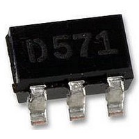
ADP1864AUJZ Analog Devices Inc, ADP1864AUJZ Datasheet

ADP1864AUJZ
Specifications of ADP1864AUJZ
Available stocks
Related parts for ADP1864AUJZ
ADP1864AUJZ Summary of contents
Page 1
FEATURES Wide input voltage range: 3. Wide output voltage range: 0 input voltage Pin-to-pin compatible with LTC1772, LTC3801 Up to 94% efficiency 0.8 V ± 1.25% reference accuracy over temperature Internal soft start 100% ...
Page 2
ADP1864 TABLE OF CONTENTS Features .............................................................................................. 1 Applications....................................................................................... 1 General Description ......................................................................... 1 Revision History ............................................................................... 2 Specifications..................................................................................... 3 Absolute Maximum Ratings............................................................ 4 ESD Caution.................................................................................. 4 Pin Configuration and Function Descriptions............................. 5 Typical Performance Characteristics ............................................. 6 Theory of Operation ...
Page 3
SPECIFICATIONS 25°C, unless otherwise noted Table 1. Parameter POWER SUPPLY Input Voltage Quiescent Current Shutdown Supply Current Undervoltage Lockout Threshold ERROR AMPLIFIER FB Input Current FB Input Current Amplifier Transconductance COMP Startup ...
Page 4
ADP1864 ABSOLUTE MAXIMUM RATINGS Table 2. Parameter IN to GND CS, PGATE to GND FB, COMP to GND θ 2-Layer (SEMI Standard Board) JA θ 4-Layer (JEDEC Standard Board) JA Operating Junction Temperature Range Storage Temperature Lead Temperature Rework Temperature ...
Page 5
PIN CONFIGURATION AND FUNCTION DESCRIPTIONS Table 3. Pin Function Descriptions Pin No. Mnemonic Description 1 COMP Regulator Compensation Node. COMP is the output of the internal transconductance error amplifier. Connect a series RC from COMP to GND to compensate for ...
Page 6
ADP1864 TYPICAL PERFORMANCE CHARACTERISTICS 0.810 0.805 0.800 0.795 0.790 –40 – TEMPERATURE (°C) Figure 4. Reference Voltage vs. Temperature 600 590 580 570 560 550 –40 –20 0 ...
Page 7
VIN = 16V 9 8 VIN = VIN = 3.15V VIN = 4V 5 –40 – TEMPERATURE (°C) Figure 10. Shutdown Supply Current vs. Temperature 310 16V 290 12V ...
Page 8
ADP1864 THEORY OF OPERATION The ADP1864 is a constant frequency (580 kHz), current-mode buck controller. PGATE drives the gate of the external P-channel FET. The duty cycle of the external FET dictates the output voltage and the current supplied to ...
Page 9
SHORT-CIRCUIT PROTECTION If there is a short across the output load, the voltage at the feedback pin (FB) drops rapidly. When the FB voltage drops below 0.35 V, the ADP1864 reduces the oscillator frequency to 190 kHz. The increase in ...
Page 10
ADP1864 APPLICATION INFORMATION DUTY CYCLE To determine the worst-case inductor ripple current, output voltage ripple, and slope compensation factor, determine the system maximum and minimum duty cycle. The duty cycle is calculated by the equation + ...
Page 11
MOSFET Choose the external P-channel MOSFET based on the following: threshold voltage (V ), maximum voltage and current ratings and gate charge. DS(ON) The minimum operating voltage of the ADP1864 is 3.15 V. Choose a MOSFET with ...
Page 12
ADP1864 LAYOUT CONSIDERATIONS Layout is important with all switching regulators, but is particu- larly important for high switching frequencies. Ensure all high current paths are as wide as possible to minimize track inductance, which causes spiking and electromagnetic inter- ference ...
Page 13
EXAMPLE APPLICATIONS CIRCUITS 470pF RSENSE LRC-LR1206_01_R030-F MOSFET FAIRCHILD SEMI FDC638P INDUCTOR TOKO FDV0630-3R3M DIODE SYNSEMI SK22 CIN LMK325BJ106KN COUT SANYO POSCAP 6TPB47M 470pF RSENSE LRC-LR1206_01_R030-F MOSFET FAIRCHILD SEMI FDC658P INDUCTOR SUMIDA CDRH6D38-5R0 DIODE VISHAY SSB43L CIN LMK325BJ106KN COUT SANYO POSCAP ...
Page 14
... ADP1864 OUTLINE DIMENSIONS INDICATOR 0.10 MAX ORDERING GUIDE Model Temperature Range 1 ADP1864AUJZ-R7 −40°C to +125°C 2 ADP1864-EVAL −40°C to +125° Pb-free part 2.5 V (variable 3. OUT LOAD IN 2.90 BSC 2.80 BSC 1.60 BSC PIN 1 0.95 BSC 1.90 * 0.90 BSC 0.87 0. ...
Page 15
NOTES Rev Page ADP1864 ...
Page 16
ADP1864 NOTES ©2005–2007 Analog Devices, Inc. All rights reserved. Trademarks and registered trademarks are the property of their respective owners. D05562-0-2/07(A) Rev Page ...


