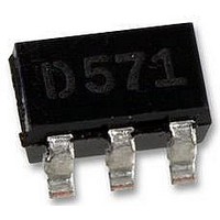
ADP1864AUJZ Analog Devices Inc, ADP1864AUJZ Datasheet - Page 8

ADP1864AUJZ
Manufacturer Part Number
ADP1864AUJZ
Description
CONTROLLER, CURRENT MODE, TSOT-6
Manufacturer
Analog Devices Inc
Datasheet
1.ADP1864AUJZ.pdf
(16 pages)
Specifications of ADP1864AUJZ
Primary Input Voltage
14V
No. Of Outputs
1
Output Voltage
14V
Output Current
5A
Voltage Regulator Case Style
TSOT
No. Of Pins
6
Operating Temperature Range
-40°C To +125°C
Svhc
No SVHC
Lead Free Status / RoHS Status
Lead free / RoHS Compliant
Available stocks
Company
Part Number
Manufacturer
Quantity
Price
Part Number:
ADP1864AUJZ
Manufacturer:
ADI/亚德诺
Quantity:
20 000
Company:
Part Number:
ADP1864AUJZ-R7
Manufacturer:
ADI
Quantity:
3 000
Part Number:
ADP1864AUJZ-R7
Manufacturer:
ADI/亚德诺
Quantity:
20 000
ADP1864
THEORY OF OPERATION
The ADP1864 is a constant frequency (580 kHz), current-mode
buck controller. PGATE drives the gate of the external P-channel
FET. The duty cycle of the external FET dictates the output
voltage and the current supplied to the load.
The peak inductor current is measured across the external sense
resistor, while the system output voltage is fed back through an
external resistor divider to the FB pin.
At the start of every oscillator cycle, PGATE turns on the
external FET, causing the inductor current, and therefore the
current sense amplifier voltage, to increase. The inductor
current increases until the current amplifier voltage equals
the voltage at the COMP pin. This resets the internal flip-flop,
causing PGATE to go high and turning off the external FET.
The inductor current decreases until the beginning of the next
oscillator period.
The voltage at the COMP node is the output of the internal
error amplifier. The negative input of the error amplifier is the
output voltage scaled by an external resistive divider, and the
VIN = 3.15V TO 14V
COMP
GND
2
1
ADP1864
UVLO
VREF
0.3V
VREF
0.8V
IN
VIN
5
FREQUENCY
FOLDBACK
4
CS
OSC
SHORT-CIRCUIT
SLOPE
COMP
15mV
DETECT
Figure 13. Functional Block Diagram
ICMP
0.6µA
Rev. A | Page 8 of 16
0.35V
R
S
RSI
0.3V
Q
SHDN
SWITCHING
LOGIC AND
BLANKING
CMP
CIRCUIT
UVLO,
positive input to the error amplifier is driven by a 0.8 V band
gap reference. An increase in the load current causes a small
drop in the feedback voltage, in turn causing an increase in the
COMP voltage and, therefore, the duty cycle. The resulting
increase in the on time of the FET provides the additional
current required by the load.
LOOP STARTUP
Pulling the COMP pin to GND disables the ADP1864. When
the COMP pin is released from GND, an internal 0.6 μA current
source charges the external compensation capacitor on the
COMP node. Once the COMP voltage has charged to 0.67 V,
the internal control blocks are enabled and COMP is pulled up
to its minimum normal operating voltage (0.9 V). As the voltage at
COMP continues to increase, the on time of the external FET
increases to supply the required inductor current. The loop
stabilizes completely once COMP voltage is sufficiently high to
support the load current. The regulation voltage at FB is 0.8 V.
UVLO
SHDN
UV
EAMP
OVP
VREF
+
80mV
VREF
0.8V
0.8V
VIN
VIN
6
3
PGATE
FB
G
S
D
2.5V
2A


