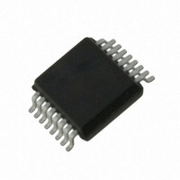
AS5043-ASST austriamicrosystems, AS5043-ASST Datasheet - Page 17

AS5043-ASST
Manufacturer Part Number
AS5043-ASST
Description
IC ENCODER PROG 10-BIT 16-SSOP
Manufacturer
austriamicrosystems
Type
Linear, Rotary Encoder - Programmabler
Datasheet
1.AS5043_PB.pdf
(36 pages)
Specifications of AS5043-ASST
Sensing Range
45mT ~ 75mT
Voltage - Supply
3 V ~ 3.6 V, 4.5 V ~ 5.5 V
Current - Supply
21mA
Current - Output (max)
4mA
Output Type
Analog, Digital
Features
Programmable
Operating Temperature
-40°C ~ 125°C
Package / Case
16-SSOP
Lead Free Status / RoHS Status
Lead free / RoHS Compliant
Other names
AS5043-ASSTTR
AS5043
Data Sheet – Programming the AS5043
Internal or external reference
The default DAC reference is the voltage at pin #16 (VDD5V) divided by 2 (see Figure 13). Using this reference, a system
that has an output voltage ratiometric to the supply voltage can be built.
Optionally, an external reference source, applied at pin#9 (DACref) can be used. This programming option is useful for
applications requiring a precise output voltage that is independent of supply fluctuations, for current sink outputs or for
applications with a dynamic reference, e.g. attenuation of audio signals.
0-100% or 10-90% full scale range
The reference voltage for the DAC is buffered internally. The recommended range for the external reference voltage is
0.2V to (VDD3V3 -0.2)V.
The DAC output voltage will be switched to 0V, when the magnetic field is out of range, when the MagInc and MagDec
indicators are both =1 and the MagRngn-pin (#1) will go low.
The default full scale output voltage range is 0-100%*VDD5V. Due to limitations in the output stage of an OP-Amp buffer,
it cannot drive the output voltage from 0-100% rail-to-rail. Without load, the minimum output voltage at 0° will be a few
millivolts higher than 0V and the maximum output voltage will be slightly lower than VDD5V. With increasing load, the
voltage drops will increase accordingly.
As a programming option, an output range of 10-90%*VDD5V can be selected. In this mode, there is no saturation at the
upper and lower output voltage limits like in the 0-100% mode and it allows failure detection as the output voltage will be
outside the 10-90% limits, when the magnetic field is in the “red” range (V
chip is interrupted (V
The unbuffered output of the DAC is accessible at pin #10 (DACout). This output must not be loaded.
12.6 OP-AMP Stage
The DAC output is buffered by a non-inverting Op-Amp stage. The amplifier is supplied by VDD5V (pin #16) and can
hence provide output voltages up to 5V.
By allowing access to the inverting input of the Op-Amp and with the addition of a few discrete components it can be
configured in many ways, like high current buffer, current sink output, adjustable angle range, etc...
Per default, the gain of the Op-Amp must be set by two external resistors (see Figure 13). Optionally, the fixed internal
gain setting (2x) may be programmed by OTP, eliminating the need for external resistors.
12.6.1 Output Noise
The Noise level at the analog output depends on two states of the digital angular output:
where:
V
TN
VDD5V
V
12.7 Application Examples
See Application Note AN5043-10 for AS5043 Application Examples.
www.austriamicrosystems.com
noise, Vout
noise,OPAMP
a)
b)
the digital angular output value is stable
In this case, the output noise is the figure given as V
for the default gain of 2x For other gains, it must be scaled accordingly.
the digital output is at the edge of a step
In this case, the digital output may jitter between two adjacent values. The rate of jitter is specified as transition
noise (parameter TN in paragraph 19.5). The resulting output noise is calculated by:
= noise level at pin Vout in Vrms
= transition noise (in °rms; see 19.5)
= Supply voltage VDD5V in V
= noise level of OPAMP
(paragraph 19.3.6) in Vrms
out
=0V or VDD5V).
V
noise
,
Vout
=
TN
Revision 1.80
∗
360
VDD
noise
5
V
in paragraph 19.3.6. Note that the noise level is given
+
V
noise
,
OPAMP
out
=0V, see Table 3) or when the supply to the
17 – 36


