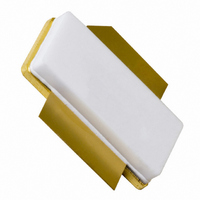
BLF6G20LS-180RN:11 NXP Semiconductors, BLF6G20LS-180RN:11 Datasheet

BLF6G20LS-180RN:11
Specifications of BLF6G20LS-180RN:11
Related parts for BLF6G20LS-180RN:11
BLF6G20LS-180RN:11 Summary of contents
Page 1
... BLF6G20-180RN; BLF6G20LS-180RN Power LDMOS transistor Rev. 01 — 17 November 2008 1. Product profile 1.1 General description 180 W LDMOS power transistor for base station applications at frequencies from 1800 MHz to 2000 MHz. Table 1. Typical RF performance at T Mode of operation 2-carrier WCDMA [1] Test signal: 3GPP; test model 1; 64 DPCH; PAR = 0.01 % probability on CCDF per carrier; ...
Page 2
... MHz to 2000 MHz frequency range 2. Pinning information Table 2. Pin BLF6G20-180RN (SOT502A BLF6G20LS-180RN (SOT502B [1] Connected to flange. 3. Ordering information Table 3. Type number BLF6G20-180RN BLF6G20LS-180RN - 4. Limiting values Table 4. In accordance with the Absolute Maximum Rating System (IEC 60134). Symbol stg T j BLF6G20-180RN_20LS-180RN_1 Product data sheet Pinning ...
Page 3
... Symbol P L(AV IMD3 ACPR 7.1 Ruggedness in class-AB operation The BLF6G20-180RN and BLF6G20LS-180RN are capable of withstanding a load mismatch corresponding to VSWR = through all phases under the following conditions: V BLF6G20-180RN_20LS-180RN_1 Product data sheet Thermal characteristics Parameter Conditions thermal resistance from T case junction to case ...
Page 4
... NXP Semiconductors 7.2 One-tone CW Fig 1. 7.3 Two-tone (dB 1400 mA 1960 MHz Fig 2. Two-tone CW power gain and drain efficiency as function of peak envelope load power; typical values BLF6G20-180RN_20LS-180RN_1 Product data sheet (dB 1400 mA 1960 MHz One-tone CW power gain and drain efficiency as function of load power; typical values ...
Page 5
... NXP Semiconductors 7.4 2-carrier W-CDMA (dB 1400 mA 1960 MHz ( 5 MHz carrier spacing 10 MHz. Fig 4. 2-carrier W-CDMA power gain and drain efficiency as function of average load power; typical values 8. Test information V GG input Fig 6. BLF6G20-180RN_20LS-180RN_1 Product data sheet 001aai654 40 IMD, ACPR D (dBc) (%) (W) L(AV) Fig 5. ...
Page 6
... NXP Semiconductors Fig 7. Table 8. List of components (see The Printed-Circuit Board (PCB) used is a double copper-clad Taconic RF35 with Component Description C1 multilayer ceramic chip capacitor C2 multilayer ceramic chip capacitor C3 multilayer ceramic chip capacitor C4 multilayer ceramic chip capacitor C5, C12, C15, C16 multilayer ceramic chip capacitor ...
Page 7
... NXP Semiconductors Table 8. List of components (see The Printed-Circuit Board (PCB) used is a double copper-clad Taconic RF35 with Component Description L1 ferrite SMD bead R1 SMD resistor R2 SMD resistor [1] Solder vertically. BLF6G20-180RN_20LS-180RN_1 Product data sheet Figure 6 and Figure 7) …continued Value - 2.7 6.8 Rev. 01 — 17 November 2008 ...
Page 8
... NXP Semiconductors 9. Package outline Flanged LDMOST ceramic package; 2 mounting holes; 2 leads DIMENSIONS (millimetre dimensions are derived from the original inch dimensions UNIT 4.72 12.83 20.02 0.15 mm 3.43 12.57 19.61 0.08 0.186 0.505 0.006 0.788 inches 0.135 0.495 0.003 0.772 OUTLINE VERSION ...
Page 9
... NXP Semiconductors Earless flanged LDMOST ceramic package; 2 leads DIMENSIONS (millimetre dimensions are derived from the original inch dimensions UNIT 4.72 12.83 20.02 0.15 mm 3.43 12.57 0.08 19.61 0.186 0.505 0.006 0.788 inches 0.495 0.135 0.003 0.772 OUTLINE VERSION IEC SOT502B Fig 9. ...
Page 10
... NXP Semiconductors 10. Abbreviations Table 9. Acronym 3GPP CCDF CDMA CW DPCH EDGE GSM LDMOS LDMOST PAR PDPCH RF VSWR W-CDMA 11. Revision history Table 10. Revision history Document ID BLF6G20-180RN_20LS-180RN_1 BLF6G20-180RN_20LS-180RN_1 Product data sheet Abbreviations Description Third Generation Partnership Project Complementary Cumulative Distribution Function Code Division Multiple Access ...
Page 11
... Right to make changes — NXP Semiconductors reserves the right to make changes to information published in this document, including without limitation specifications and product descriptions, at any time and without notice ...
Page 12
... NXP Semiconductors 14. Contents 1 Product profi 1.1 General description 1.2 Features . . . . . . . . . . . . . . . . . . . . . . . . . . . . . . 1 1.3 Applications . . . . . . . . . . . . . . . . . . . . . . . . . . . 2 2 Pinning information . . . . . . . . . . . . . . . . . . . . . . 2 3 Ordering information . . . . . . . . . . . . . . . . . . . . . 2 4 Limiting values Thermal characteristics Characteristics . . . . . . . . . . . . . . . . . . . . . . . . . . 3 7 Application information 7.1 Ruggedness in class-AB operation 7.2 One-tone 7.3 Two-tone 7.4 2-carrier W-CDMA . . . . . . . . . . . . . . . . . . . . . . 5 8 Test information . . . . . . . . . . . . . . . . . . . . . . . . . 5 9 Package outline ...


