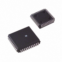
AD8600APZ Analog Devices Inc, AD8600APZ Datasheet - Page 10

AD8600APZ
Manufacturer Part Number
AD8600APZ
Description
16 CHANNEL 8-BIT MULT.DAC
Manufacturer
Analog Devices Inc
Datasheet
1.AD8600APZ-REEL.pdf
(16 pages)
Specifications of AD8600APZ
Rohs Compliant
YES
Settling Time
1µs
Number Of Bits
8
Data Interface
Parallel
Number Of Converters
16
Voltage Supply Source
Analog and Digital, Dual ±
Power Dissipation (max)
175mW
Operating Temperature
-40°C ~ 85°C
Mounting Type
Surface Mount
Package / Case
44-PLCC
Lead Free Status / RoHS Status
Lead free / RoHS Compliant
Available stocks
Company
Part Number
Manufacturer
Quantity
Price
Company:
Part Number:
AD8600APZ
Manufacturer:
Analog Devices Inc
Quantity:
10 000
Part Number:
AD8600APZ
Manufacturer:
ADI/亚德诺
Quantity:
20 000
Company:
Part Number:
AD8600APZ-REEL
Manufacturer:
Analog Devices Inc
Quantity:
10 000
AD8600
Interface Timing and Control
The AD8600 employs a double buffered DAC structure with
each DAC channel having a unique input register and DAC reg-
ister as shown in the diagram entitled “Equivalent DAC Chan-
nel” on the first page of the data sheet. This structure allows
maximum flexibility in loading the DACs. For example, each
DAC can be updated independently, or, if desired, all 16 input
registers can be loaded, followed by a single LD strobe to up-
date all 16 DACs simultaneously. An additional feature is the
ability to read back from the input register to verify the DAC’s
data.
The interface logic for a single DAC channel is shown in Figure
19. This figure specifically shows the logic for Channel 0; how-
ever, by changing the address input configuration to gate N1,
the other 15 channels are achieved. All of the logic for the
AD8600 is level sensitive and not edge triggered. For example,
if all the control inputs (CS, R/W, EN, LD) are low, the input
and DAC registers are transparent and any change in the digital
inputs will immediately change the DAC’s R-2R ladder.
Table I details the different logic combinations and their effects.
Chip Select (CS), Enable (EN) and R/W must be low to write
the input register. During this time that all three are low, any
data on DB7–DB0 changes the contents of the input register.
This data is not latched until either EN or CS returns high.
The data setup and hold times shown in the timing diagrams
must be observed to ensure that the proper data is latched into
the input register.
D7–D0
R/W
R/W
Figure 19. Logic Interface Circuit for DAC Channel 0
EN
CS
CS
EN
LD
A0
A1
A2
A3
N1
N2
N3
N4
8
8
N5
N6
READ BACK
REGISTER
INPUT
8
REGISTER
DAC
R-2R
LADDER
–10–
To load multiple input registers in the fastest time possible,
both R/W and CS should remain low, and the EN line be used
to “clock” in the data. As the write timing diagram shows, the
address should be updated at the same time as EN goes low.
Before EN returns high, valid data must be present for a time
equal to the data setup time (t
the data Hold Time (t
mum times are violated, invalid data may be latched into the in-
put register. This cycle can be repeated 16 times to load all of
the DACs. The fastest interface time is equal to the sum of the
low and high times (t
minimum of 80 ns. Because the EN input is used to clock in
the data, it is often referred to as the clock input, and the timing
specifications give a maximum clock frequency of 12.5 MHz,
which is just the reciprocal of 80 ns.
After all the input registers have been loaded, a single load
strobe will transfer the contents of the input registers to the
DAC registers. EN must also be low during this time. If the
address or data on the inputs could change, then CS should be
high during this time to ensure that new data is not loaded into
an input register. Alternatively, a single DAC can be updated
by first loading its input register and then transferring that to the
DAC register without loading the other 15 input registers.
The final interface option is to read data from the DAC’s input
registers, which is accomplished by setting R/W high and bring-
ing CS low. Read back allows the microprocessor to verify that
correct data has been loaded into the DACs. During this time
EN and LD should be high. After a delay equal to t
data bus becomes active and the contents of the input register
are read back to the data pins, DB0–DB7. The address can be
changed to look at the contents of all the input registers. Note
that after an address change, the valid data is not available for a
time equal to t
readback buffers needing to charge up the data bus (measured
with a 35 pF load). These buffers are low power and do not
have high current to charge the bus quickly. When CS returns
high, the data pins assume a high impedance state and control
of the data lines or bus passes back to the microprocessor.
AD
. The delay time is due to the internal
CL
DH
and t
) must be maintained. If these mini-
CH
DS
) for the EN input, which gives a
), and after EN returns high,
RWD
, the
REV. 0


