AD8600APZ Analog Devices Inc, AD8600APZ Datasheet - Page 9
AD8600APZ
Manufacturer Part Number
AD8600APZ
Description
16 CHANNEL 8-BIT MULT.DAC
Manufacturer
Analog Devices Inc
Datasheet
1.AD8600APZ-REEL.pdf
(16 pages)
Specifications of AD8600APZ
Rohs Compliant
YES
Settling Time
1µs
Number Of Bits
8
Data Interface
Parallel
Number Of Converters
16
Voltage Supply Source
Analog and Digital, Dual ±
Power Dissipation (max)
175mW
Operating Temperature
-40°C ~ 85°C
Mounting Type
Surface Mount
Package / Case
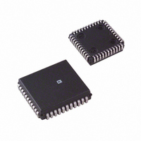
44-PLCC
Lead Free Status / RoHS Status
Lead free / RoHS Compliant
Available stocks
Company
Part Number
Manufacturer
Quantity
Price
Company:

Part Number:
AD8600APZ
Manufacturer:
Analog Devices Inc
Quantity:
10 000
Part Number:
AD8600APZ
Manufacturer:
ADI/亚德诺
Quantity:
20 000
Company:
Part Number:
AD8600APZ-REEL
Manufacturer:
Analog Devices Inc
Quantity:
10 000


REV. 0
Power Supply and Grounding Considerations
The low power consumption of the AD8600 is a direct result of
circuit design optimizing using a CBCMOS process. The over-
all power dissipation of 120 mW translates to a total supply cur-
rent of only 24 mA for 16 DACs. Thus, each DAC consumes
only 1.5 mA. Because the digital interface is comprised entirely
of CMOS logic, the power dissipation is dependent upon the
logic input levels. As expected for CMOS, the lowest power
dissipation is achieved when the input level is either close to
ground or +5 V. Thus, to minimize the power consumption,
CMOS logic should be used to interface to the AD8600.
The AD8600 has multiple supply pins. V
the output amplifiers’ positive supply, and V
the amplifiers’ negative supply. The digital input circuitry is
powered by V
2R ladder switches are powered by V
noise feedthrough from the supplies, each supply pin should be
decoupled with a 0.1 F ceramic capacitor close to the pin.
When applying power to the device, it is important for the digi-
tal supply, V
for V
operation. Otherwise, an inherent diode will energize, and it
could damage the AD8600.
In order to improve ESD resistance, the AD8600 has several
ESD protection diodes on its various pins. These diodes shunt
ESD energy to the power supplies and protect the sensitive ac-
tive circuitry. During normal operation, all the ESD diodes are
reversed biased and do not affect the part. However, if overvolt-
ages occur on the various inputs, these diodes will energize. If
the overvoltage is due to ESD, the electrical spike is typically
short enough so that the part is not damaged. However, if the
overvoltage is continuous and has sufficient current, the part
could be damaged. To protect the part, it is important not to
forward bias any of the ESD protection diodes during normal
operation or during power up. Figure 18 shows the location of
these diodes. For example, the digital inputs have diodes con-
nected to V
digital input should never exceed the analog supply or drop be-
low ground, which is also indicated in the absolute maximum
ratings.
REF
to remain less than 0.3 V above V
CC
DD2
DD1
and from DGND1. Thus, the voltage on any
, to power on before the reference voltage and
(Pin 14), and finally the DAC register and R-
DD2
(Pin 44). To minimize
CC
DD2
EE
(Pins 4 and 42) is
during normal
(Pins 5 and 41)
–9–
Attention should be paid to the ground pins of the AD8600 to
ensure that noise is not introduced to the output. The pin la-
beled DACGND (Pin 3) is actually the ground for the R-2R
ladder, and because of this, it is important to connect this pin to
a high quality analog ground. Ideally, the analog ground should
be an actual ground plane. This helps create a low impedance,
low noise ground to maintain accuracy in the analog circuitry.
The digital ground pins (DGND1 at Pin 32 and DGND2 at
Pin 43) provide the ground reference for the internal digital cir-
cuitry and latches. The first thought may be to connect both of
these pins to the system digital ground. However, this is not the
best choice because of the high noise typically found on a
system’s digital ground. This noise can feed through to the out-
put through the DAC’s ground pins. Instead, DGND1 and
DGND2 should be connected to the analog ground plane. The
actual switching current in these pins is small and should not
degrade the analog ground.
5 V Output Swing
The output swing is limited to 1.0 V below the positive supply.
This gives a maximum output of +4.0 V on a +5 V supply. To
increase the output range, the analog supply, V
ladder supply, V
output of +5 V with a 5 V reference. V
+5 V to ensure that the input logic levels do not change.
Reference Input Considerations
The AD8600 is designed for one reference to drive all 16 DACs.
The reference pin (V
ders of each DAC. With 16 DACs in parallel, the input imped-
ance is typically 2 k and a minimum of 1.2 k . The input
resistance is code dependent. Thus, the chosen reference device
must be able to drive this load. Some examples of +2.5 V refer-
ences that easily interface to the AD8600 are the REF43,
AD680, and AD780. The unique architecture ensures that the
reference does not have to supply “shoot through” current,
which is a condition in some voltage mode DACs where the ref-
erence is momentarily connected to ground through the CMOS
switches. By eliminating this possibility, all 16 DACs in the
AD8600 can easily be driven from a single reference.
Figure 18. ESD Protection Diode Locations
(R/W, CS, EN, LD, RS)
ALL DIGITAL INPUTS
DD2
(A0–A3, DB0–DB7)
, can be increased to +7 V. This allows an
REF
) is connected directly to the R-2R lad-
V
REF
DGND1
DACGND
DD1
V
CC
should remain at
V
CC
DD2
AD8600
, and the DAC
Related parts for AD8600APZ
Image
Part Number
Description
Manufacturer
Datasheet
Request
R

Part Number:
Description:
±1.7g Dual-Axis IMEMS Accelerometer Evaluation Board
Manufacturer:
Analog Devices Inc
Datasheet:

Part Number:
Description:
Inertial Sensor Evaluation System
Manufacturer:
Analog Devices Inc
Datasheet:
Part Number:
Description:
Manufacturer:
Analog Devices Inc
Datasheet:
Part Number:
Description:
Manufacturer:
Analog Devices Inc
Datasheet:
Part Number:
Description:
Manufacturer:
Analog Devices Inc
Datasheet:
Part Number:
Description:
Manufacturer:
Analog Devices Inc
Datasheet:
Part Number:
Description:
Manufacturer:
Analog Devices Inc
Datasheet:
Part Number:
Description:
Manufacturer:
Analog Devices Inc
Datasheet:
Part Number:
Description:
Manufacturer:
Analog Devices Inc
Datasheet:
Part Number:
Description:
Manufacturer:
Analog Devices Inc
Datasheet:
Part Number:
Description:
Manufacturer:
Analog Devices Inc
Datasheet:
Part Number:
Description:
Manufacturer:
Analog Devices Inc
Datasheet:
Part Number:
Description:
Manufacturer:
Analog Devices Inc
Datasheet: