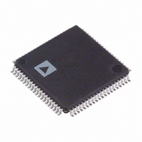
AD9980KSTZ-80 Analog Devices Inc, AD9980KSTZ-80 Datasheet - Page 38

AD9980KSTZ-80
Manufacturer Part Number
AD9980KSTZ-80
Description
IC,Data Acquisition Signal Conditioner,3-CHANNEL,8-BIT,CMOS,QFP,80PIN,PLASTIC
Manufacturer
Analog Devices Inc
Datasheet
1.AD9980KSTZ-80.pdf
(44 pages)
Specifications of AD9980KSTZ-80
Applications
Video
Interface
Analog
Voltage - Supply
3.13 V ~ 3.47 V
Package / Case
80-LQFP
Mounting Type
Surface Mount
Lead Free Status / RoHS Status
Lead free / RoHS Compliant
For Use With
AD9980/PCBZ - KIT EVALUATION AD9980
Lead Free Status / RoHS Status
Lead free / RoHS Compliant
Available stocks
Company
Part Number
Manufacturer
Quantity
Price
Company:
Part Number:
AD9980KSTZ-80
Manufacturer:
ADI
Quantity:
830
Company:
Part Number:
AD9980KSTZ-80
Manufacturer:
Analog Devices Inc
Quantity:
10 000
Part Number:
AD9980KSTZ-80
Manufacturer:
ADI/亚德诺
Quantity:
20 000
AD9980
TWO-WIRE SERIAL CONTROL PORT
A two-wire serial interface control interface is provided. Up to
two AD9980 devices may be connected to the two-wire serial
interface with each device having a unique address.
The two-wire serial interface comprises a clock (SCL) and a bi-
directional data pin (SDA). The analog flat panel interface acts
as a slave for receiving and transmitting data over the serial
interface. When the serial interface is not active, the logic levels
on SCL and SDA are pulled high by external pull-up resistors.
Data received or transmitted on the SDA line must be stable for
the duration of the positive going SCL pulse. Data on SDA must
change only when SCL is low. If SDA changes state while SCL is
high, the serial interface interprets that action as a start or stop
sequence.
The following are the five components to serial bus operation:
•
•
•
•
•
When the serial interface is inactive (SCL and SDA are high),
communication is initiated by sending a start signal. The start
signal is a high-to-low transition on SDA while SCL is high.
This signal alerts all slaved devices that a data transfer sequence
is coming.
The first eight bits of data transferred after a start signal
comprise a 7-bit slave address (the first seven bits) and a single
R/W\ bit (the eighth bit). The R/W\ bit indicates the direction
of data transfer: read from 1 or write to 0 on the slave device. If
the transmitted slave address matches the address of the device
(set by the state of the Serial A0 address [SA0] input pin in
Table 76), the AD9980 acknowledges the match by bringing
SDA low on the ninth SCL pulse. If the addresses do not match,
the AD9980 does not acknowledge it.
Start signal
Slave address byte
Base register address byte
Data byte to read or write
Stop signal
SDA
SCL
t
STAH
t
BUFF
t
DHO
t
DAL
Figure 17. Serial Port Read/Write Timing
t
DAH
t
DSU
Rev. 0 | Page 38 of 44
Table 76. Serial Port Addresses
Bit 7
A6 (MSB)
1
1
DATA TRANSFER VIA SERIAL INTERFACE
For each byte of data read or written, the MSB is the first bit in
the sequence.
If the AD9980 does not acknowledge the master device during a
write sequence, the SDA remains high so the master can gener-
ate a stop signal. If the master device does not acknowledge the
AD9980 during a read sequence, the AD9980 interprets this as
end-of-data. The SDA remains high so the master can generate
a stop signal.
Writing data to specific control registers of the AD9980 requires
that the 8-bit address of the control register of interest be writ-
ten after the slave address has been established. This control
register address is the base address for subsequent write opera-
tions. The base address auto-increments by one for each byte of
data written after the data byte intended for the base address. If
more bytes are transferred than there are available addresses,
the address will not increment and remains at its maximum
value of 0x2E. Any base address higher than 0x2E does not pro-
duce an acknowledge signal. Data are read from the control
registers of the AD9980 in a similar manner. Reading requires
two data transfer operations:
The base address must be written with the R/W bit of the slave
address byte low to set up a sequential read operation. Reading
(the R/W\ bit of the slave address byte high) begins at the
previously established base address. The address of the read
register auto-increments after each byte is transferred.
To terminate a read/write sequence to the AD9980, a stop signal
must be sent. A stop signal comprises a low-to-high transition
of SDA while SCL is high.
A repeated start signal occurs when the master device driving
the serial interface generates a start signal without first gener-
ating a stop signal to terminate the current communication.
This is used to change the mode of communication (read, write)
between the slave and master without releasing the serial
interface lines.
t
STASU
Bit 6
A5
0
0
Preliminary Technical Data
Bit 5
A4
0
0
t
STOSU
Bit 4
A3
1
1
Bit 3
A2
1
1
Bit 2
A1
0
0
Bit 1
A0
0
1


