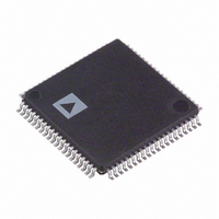
AD9980KSTZ-80 Analog Devices Inc, AD9980KSTZ-80 Datasheet - Page 9

AD9980KSTZ-80
Manufacturer Part Number
AD9980KSTZ-80
Description
IC,Data Acquisition Signal Conditioner,3-CHANNEL,8-BIT,CMOS,QFP,80PIN,PLASTIC
Manufacturer
Analog Devices Inc
Datasheet
1.AD9980KSTZ-80.pdf
(44 pages)
Specifications of AD9980KSTZ-80
Applications
Video
Interface
Analog
Voltage - Supply
3.13 V ~ 3.47 V
Package / Case
80-LQFP
Mounting Type
Surface Mount
Lead Free Status / RoHS Status
Lead free / RoHS Compliant
For Use With
AD9980/PCBZ - KIT EVALUATION AD9980
Lead Free Status / RoHS Status
Lead free / RoHS Compliant
Available stocks
Company
Part Number
Manufacturer
Quantity
Price
Company:
Part Number:
AD9980KSTZ-80
Manufacturer:
ADI
Quantity:
830
Company:
Part Number:
AD9980KSTZ-80
Manufacturer:
Analog Devices Inc
Quantity:
10 000
Part Number:
AD9980KSTZ-80
Manufacturer:
ADI/亚德诺
Quantity:
20 000
Pin
OUTPUTS
SERIAL PORT
DATA OUTPUTS
DATA CLOCK OUTPUT
POWER SUPPLY
FILT
HSOUT
VSOUT/A0
SOGOUT
O/E FIELD
SDA
SCL
VSOUT/A0
RED [7:0]
GREEN [7:0]
BLUE [7:0]
DATACK
V
V
PV
DAV
GND
D
DD
D
(3.3 V)
(1.8 V to 3.3 V)
(1.8 V)
DD
(1.8 V)
Description
External Filter Connection. For proper operation, the pixel clock generator PLL requires an external filter.
Connect the filter shown in Figure 7 to this pin. For optimal performance, minimize noise and parasitics on this
node. For more information see the PCB Layout Recommendations section.
Horizontal Sync Output. A reconstructed and phase-aligned version of the Hsync input. Both the polarity and
duration of this output can be programmed via serial bus registers. By maintaining alignment with DATACK and
Data Outputs, data timing with respect to Hsync can always be determined.
Vertical Sync Output. Pin shared with A0, serial port address. This can be either a separated Vsync from a
composite signal or a direct pass through of the Vsync signal. The polarity of this output can be controlled via a
serial bus bit. The placement and duration in all modes can be set by the graphics transmitter or the duration
can be set by Register 0x14 and Register 0x15. This pin is shared with the A0 function, which does not affect
Vsync output functionality. For more details on A0, see the description in the Serial Control Port section.
Sync-On-Green Slicer Output. This pin outputs one of four possible signals (controlled by Register 0x1D,
Bits [1:0]): raw SOG, raw Hsync, regenerated Hsync from the filter, or the filtered Hsync. See the sync processing
block diagram (Figure 8) to view how this pin is connected. (Besides slicing off SOG, the output from this pin gets
no other additional processing on the AD9980. Vsync separation is performed via the sync separator.)
Odd/Even Field Bit for Interlaced Video.
This output will identify whether the current field (in an interlaced signal) is odd or even.
Serial Port Data I/O.
Serial Port Data Clock.
Serial Port Address Input 0. Pin shared with VSOUT. This pin selects the LSB of the serial port device address,
allowing two Analog Devices parts to be on the same serial bus. A high impedance external pull-up resistor
enables this pin to be read at power-up as 1, or a high impedance, external pull-down resistor enables this pin to
be read at power-up as a 0 and not interfere with the VSOUT functionality. For more details on VSOUT, see the
Outputs section in this table.
Data Output, Red Channel.
Data Output, Green Channel.
Data Output, Blue Channel.
The main data outputs. Bit 7 is the MSB. The delay from pixel sampling time to output is fixed. When the
sampling time is changed by adjusting the phase register, the output timing is shifted as well. The DATACK and
HSOUT outputs are also moved, so the timing relationship among the signals is maintained.
Data Clock Output. This is the main clock output signal used to strobe the output data and HSOUT into external
logic. Four possible output clocks can be selected with Register 0x20, Bits [7:6]. Three of these are related to the
pixel clock (pixel clock, 90° phase-shifted pixel clock, and 2× frequency pixel clock). They are produced either by
the internal PLL clock generator or EXTCLK and are synchronous with the pixel sampling clock. The fourth option
for the data clock output is an internally generated 40 MHz clock.
The sampling time of the internal pixel clock can be changed by adjusting the phase register (Register 0x04).
When this is changed, the pixel related DATACK timing is also shifted. The Data, DATACK, and HSOUT outputs
are all moved so that the timing relationship among the signals is maintained.
Main Power Supply. These pins supply power to the main elements of the circuit. They should be as quiet and
filtered as possible.
Digital Output Power Supply. A large number of output pins (up to 29) switching at high speed (up to 95 MHz)
generate a lot of power supply transients (noise). These supply pins are identified separately from the V
special care can be taken to minimize output noise transferred into the sensitive analog circuitry. If the AD9980
is interfacing with lower voltage logic, V
compatibility.
Clock Generator Power Supply. The most sensitive portion of the AD9980 is the clock generation circuitry. These
pins provide power to the clock PLL and help the user design for optimal performance. The designer should
provide quiet, noise-free power to these pins.
Digital Input Power Supply. This supplies power to the digital logic.
Ground. The ground return for all circuitry on-chip. It is recommended that the AD9980 be assembled on a
single solid ground plane, with careful attention to ground current paths.
Rev. 0 | Page 9 of 44
DD
may be connected to a lower supply voltage (as low as 1.8 V) for
AD9980
D
pins, so


