CY7C4271-15AXC Cypress Semiconductor Corp, CY7C4271-15AXC Datasheet
CY7C4271-15AXC
Specifications of CY7C4271-15AXC
Available stocks


Related parts for CY7C4271-15AXC


CY7C4271-15AXC Summary of contents
Page 1
... K × 9 Deep Sync FIFOs Features High speed, low power, first-in first-out (FIFO) memories ■ × 9 (CY7C4261) ■ × 9 (CY7C4271) ■ 0.5 micron CMOS for optimum speed and power ■ High speed 100 MHz operation (10 ns read/write cycle times) ■ Low power — ■ ...
Page 2
... WRITE POINTER RESET RS LOGIC Document Number: 38-06015 Rev 0–8 INPUT REGISTER WEN2/ LD RAM ARRAY 16K x 9 32K x 9 THREE-STATE OUTPUT REGISTER OE Q 0–8 RCLK CY7C4261, CY7C4271 FLAG PROGRAM REGISTER EF PAE FLAG LOGIC PAF FF READ POINTER READ CONTROL REN1 REN2 Page [+] Feedback ...
Page 3
... Width Expansion Configuration ...................................... 6 Flag Operation .................................................................. 6 Full Flag ....................................................................... 6 Empty Flag .................................................................. 6 Maximum Ratings ............................................................. 8 Operating Range ............................................................... 8 Electrical Characteristics ................................................. 8 Document Number: 38-06015 Rev. *G CY7C4261, CY7C4271 Capacitance ...................................................................... 8 Switching Characteristics ................................................ 9 Switching Waveforms .................................................... 10 Ordering Information ...................................................... × 9 Deep Sync FIFO ......................................... × 9 Deep Sync FIFO ......................................... 16 Ordering Code Definitions ......................................... 16 Package Diagrams .......................................................... 18 Document History Page ...
Page 4
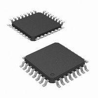
... HIGH, the FIFO’s outputs are in high Z (high impedance) state. Document Number: 38-06015 Rev. *G Figure 2. Pin Diagram - 32-pin TQFP (Top View WEN1 D 0 WCLK PAF LD WEN2/ PAE V CC GND REN1 7 Q RCLK REN2 Description CY7C4261, CY7C4271 WEN1 2 23 WCLK 3 WEN2/ CY7C4271 ...
Page 5
... Empty Offset (LSB) Reg. Default Value = 007h 8 08 outputs after 0 Full Offset (LSB) Reg Default Value = 007h 8 outputs even 08 CY7C4261, CY7C4271 Figure 3 shows the register sizes and default 32K × Empty Offset (LSB) Reg. Default Value = 007h (MSB) (MSB) ...
Page 6
... PAF. PAF is synchronized to the LOW-to-HIGH transition of WCLK by one flip-flop and is set LOW when the number of unread words in the FIFO is greater than or equal to CY7C4261 (16K-m) and CY7C4271 (32K-m). PAF is set HIGH by the LOW-to-HIGH transition of WCLK when the number of available memory locations is greater than m. ...
Page 7
... PROGRAMMABLE(PAF) FULL FLAG (FF FULL FLAG (FF Read Enable 2 (REN2) Document Number: 38-06015 Rev. *G RESET (RS) RESET (RS) 9 CY7C4261/71 CY7C4261/ Read Enable 2 (REN2) CY7C4261, CY7C4271 READ CLOCK (RCLK) READ ENABLE 1 (REN1) OUTPUT ENABLE (OE) PROGRAMMABLE(PAE) EMPTY FLAG (EF) #1 EMPTY FLAG (EF DATA OUT ( Page [+] Feedback ...
Page 8
... Min 8 Max CC OE < V < Commercial Industrial/Military Commercial Industrial/Military Test Conditions MHz 5 CY7C4261, CY7C4271 V CC 10 +70 C 10 +85 C 10 +125 C 7C4261/71-10 7C4261/71-15 Unit Min Max Min Max 2.4 – 2.4 – ...
Page 9
... Pulse widths less than minimum values are not allowed. 13. Values guaranteed by design, not currently tested. Document Number: 38-06015 Rev. *G Figure 5. AC Test Loads and Waveforms R1 1.1K 3.0 V GND R2 680 1.91 V Description [13] [13] . CY7C4261, CY7C4271 [10, 11] ALL INPUT PULSES 90% 90% 10% 10% 3 ns 7C4261/71-10 7C4261/71-15 Min Max Min Max – ...
Page 10
... NO OPERATION t REF t A VALID DATA t OE [15] t SKEW1 , then FF may not change state until the next WCLK rising edge. SKEW1 , then EF may not change state until the next RCLK rising edge. SKEW2 CY7C4261, CY7C4271 NO OPERATION NO OPERATION t WFF t REF t OHZ Page [+] Feedback ...
Page 11
... Document Number: 38-06015 Rev. *G [16] Figure 8. Reset Timing RSS t t RSS t t RSS t RSF t RSF t RSF [19] t FRL t SKEW1 t REF [20 OLZ When t < minimum specification, t CLK SKEW2 SKEW2 CY7C4261, CY7C4271 RSR RSR RSR [17 (maximum) = either 2 × FRL CLK SKEW1 Page CLK [+] Feedback ...
Page 12
... DATA WRITE t WFF t ENH t A DATA READ + t . When t < minimum specification, t CLK SKEW2 SKEW2 , then FF may not change state until the next WCLK rising edge. SKEW1 CY7C4261, CY7C4271 DATA WRITE 2 t ENH ENS t ENH ENS [21] t FRL t t REF SKEW1 NO WRITE ...
Page 13
... If a write is performed on this rising edge of the write clock, there are Full (m1) words of the FIFO when PAF goes LOW. 27. PAF offset = m. 28. 16,384 m words for CY7C4261, 32,768 m words for CY7C4271. 29 the minimum time between a rising RCLK edge and a rising WCLK edge for PAF to change during that clock cycle. If the time between the rising edge of ...
Page 14
... Figure 14. Write Programmable Registers t CLKL t ENH t DH PAE OFFSET PAF OFFSET LSB MSB Figure 15. Read Programmable Registers t CLKL t ENH t A UNKNOWN PAE OFFSET LSB CY7C4261, CY7C4271 PAF OFFSET LSB MSB PAF OFFSET MSB PAF OFFSET PAE OFFSET MSB LSB Page [+] Feedback ...
Page 15
... AMBIENT TEMPERATURE ( C) NORMALIZED SUPPLY CURRENT vs. AMBIENT TEMPERATURE 1.20 1.10 1. 3. MHz 0.80 55.00 5.00 65.00 125.00 AMBIENT TEMPERATURE ( C) CY7C4261, CY7C4271 vs. AMBIENT 5.0V CC 5.00 65.00 125.00 NORMALIZED SUPPLY CURRENT vs. FREQUENCY 1.75 1.50 1. 3.0V IN 0.50 20 ...
Page 16
... Ordering Information 16 K × 9 Deep Sync FIFO Speed (ns) Ordering Code Package Diagram 10 CY7C4261-10JXI 32 K × 9 Deep Sync FIFO Speed (ns) Ordering Code Package Diagram 15 CY7C4271-15AXC Ordering Code Definitions CY7C 42X1 - Table 4. DC Characteristics Parameters Max CC1 I SB1 I SB2 I OS Document Number: 38-06015 Rev. *G ...
Page 17
... PRT t RTR t EFL t HFH t FFH t REF t RFF t WEF t WFF t WHF t RHF t RAE t RPE t WAF t WPF t XOL t XOH Document Number: 38-06015 Rev. *G CY7C4261, CY7C4271 Subgroups 10, 11 ...
Page 18
... Package Diagrams Figure 17. 32-pin Thin Plastic Quad Flatpack (7 × 7 × 1.0 mm) Document Number: 38-06015 Rev. *G CY7C4261, CY7C4271 51-85063 *C Page [+] Feedback ...
Page 19
... Document Number: 38-06015 Rev. *G Figure 18. 32-pin Plastic Leaded Chip Carrier CY7C4261, CY7C4271 51-85002 *C Page [+] Feedback ...
Page 20
... LOW when the number of unread words in the FIFO is greater than or equal to CY7C4261 (16K-m) and CY7C4271 (32K-m).” to read as “PAF is synchronized to the LOW-to-HIGH transition of WCLK by one flip-flop and is set LOW when the number of unread words in the FIFO is greater than or equal to CY7C4261 (16K-m) and CY7C4271 (32K-m).” Updated Electrical Characteristics. Removed information for speed pins 25 ■ ...
Page 21
... Cypress against all charges. Use may be limited by and subject to the applicable Cypress software license agreement. Document Number: 38-06015 Rev. *G All products and company names mentioned in this document may be the trademarks of their respective holders. cypress.com/go/plc Revised November 2, 2010 CY7C4261, CY7C4271 PSoC Solutions psoc.cypress.com/solutions PSoC 1 | PSoC 3 ...