CY7C4271-15AXC Cypress Semiconductor Corp, CY7C4271-15AXC Datasheet - Page 4
CY7C4271-15AXC
Manufacturer Part Number
CY7C4271-15AXC
Description
CY7C4271-15AXC
Manufacturer
Cypress Semiconductor Corp
Series
CY7Cr
Datasheet
1.CY7C4261-10JXI.pdf
(21 pages)
Specifications of CY7C4271-15AXC
Function
Synchronous
Memory Size
288K (32K x 9)
Data Rate
100MHz
Access Time
10ns
Voltage - Supply
3.3V
Operating Temperature
-40°C ~ 85°C
Mounting Type
Surface Mount
Package / Case
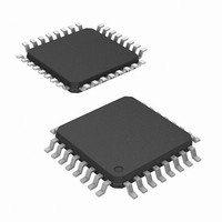
32-TQFP
Lead Free Status / RoHS Status
Lead free / RoHS Compliant
Available stocks
Company
Part Number
Manufacturer
Quantity
Price
Company:

Part Number:
CY7C4271-15AXC
Manufacturer:
Cypress Semiconductor Corp
Quantity:
10 000


Pinouts
Table 1. Pin Definitions - 32-pin Device
Document Number: 38-06015 Rev. *G
D
Q
WEN1
WEN2/LD
Dual Mode Pin
REN1, REN2
WCLK
RCLK
EF
FF
PAE
PAF
RS
OE
Signal Name
08
8
Figure 1. Pin Diagram - 32-pin PLCC (Top View)
REN1
RCLK
REN2
GND
PAE
PAF
Data inputs
Data outputs
Write enable 1
Write enable 2
Load
Read enable
inputs
Write clock
Read clock
Empty flag
Full flag
Programmable
almost empty
Programmable
almost full
Reset
Output enable
OE
D
D
1
0
Description
5
6
7
8
9
10
11
12
13
14 15 16 17 18 19 20
4 3 2 1
CY7C4261
32
31 30
IO
O
O
O
O
O
I
I
I
I
I
I
I
I
29
28
27
26
25
24
23
22
21
Data inputs for 9-bit bus.
Data outputs for 9-bit bus.
The only write enable when device is configured to have programmable flags. Data is written
on a LOW-to-HIGH transition of WCLK when WEN1 is asserted and FF is HIGH. If the FIFO
is configured to have two write enables, data is written on a LOW-to-HIGH transition of WCLK
when WEN1 is LOW and WEN2/LD and FF are HIGH.
If HIGH at reset, this pin operates as a second write enable. If LOW at reset, this pin operates
as a control to write or read the programmable flag offsets. WEN1 must be LOW and WEN2
must be HIGH to write data into the FIFO. Data is not written into the FIFO if the FF is LOW.
If the FIFO is configured to have programmable flags, WEN2/LD is held LOW to write or read
the programmable flag offsets.
Enables the device for read operation. Both REN1 and REN2 must be asserted to allow a
read operation.
The rising edge clocks data into the FIFO when WEN1 is LOW and WEN2/LD is HIGH and
the FIFO is not full. When LD is asserted, WCLK writes data into the programmable flag-offset
register.
The rising edge clocks data out of the FIFO when REN1 and REN2 are LOW and the FIFO
is not empty. When WEN2/LD is LOW, RCLK reads data out of the programmable flag-offset
register.
When EF is LOW, the FIFO is empty. EF is synchronized to RCLK.
When FF is LOW, the FIFO is full. FF is synchronized to WCLK.
When PAE is LOW, the FIFO is almost empty based on the almost empty offset value
programmed into the FIFO. PAE is synchronized to RCLK.
When PAF is LOW, the FIFO is almost full based on the almost full offset value programmed
into the FIFO. PAF is synchronized to WCLK.
Resets device to empty condition. A reset is required before an initial read or write operation
after power-up.
When OE is LOW, the FIFO’s data outputs drive the bus to which they are connected. If OE
is HIGH, the FIFO’s outputs are in high Z (high impedance) state.
RS
WEN1
WCLK
WEN2/
V
Q
Q
Q
Q
CC
8
7
6
5
LD
Figure 2. Pin Diagram - 32-pin TQFP (Top View)
REN1
RCLK
REN2
Description
GND
PAE
PAF
D
D
1
0
1
2
3
4
5
6
7
8
32
9 10 11 12 13
31 30
CY7C4261, CY7C4271
CY7C4271
29 28 27
14 15 16
26
25
24
23
22
21
20
19
18
17
WEN1
WCLK
WEN2/LD
V
Q
Q
Q
Q
CC
8
7
6
5
Page 4 of 21
[+] Feedback
Related parts for CY7C4271-15AXC
Image
Part Number
Description
Manufacturer
Datasheet
Request
R

Part Number:
Description:
IC FIFO 32KX9 SYNCHRONOUS 32QFP
Manufacturer:
Cypress Semiconductor Corp
Datasheet:

Part Number:
Description:
IC DEEP SYNC FIFO 32KX9 32-PLCC
Manufacturer:
Cypress Semiconductor Corp
Datasheet:
Part Number:
Description:
Manufacturer:
Cypress Semiconductor Corp
Datasheet:

Part Number:
Description:
Manufacturer:
Cypress Semiconductor Corp
Datasheet:
Part Number:
Description:
Manufacturer:
Cypress Semiconductor Corp
Datasheet:
Part Number:
Description:
Manufacturer:
Cypress Semiconductor Corp
Datasheet:
Part Number:
Description:
Manufacturer:
Cypress Semiconductor Corp
Datasheet:
Part Number:
Description:
Manufacturer:
Cypress Semiconductor Corp
Datasheet: