UBA2024BP/N1,112 NXP Semiconductors, UBA2024BP/N1,112 Datasheet - Page 4
UBA2024BP/N1,112
Manufacturer Part Number
UBA2024BP/N1,112
Description
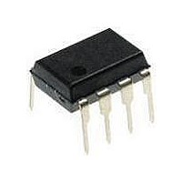
IC DRIVER HALF BRIDGE 8-DIP
Manufacturer
NXP Semiconductors
Type
CFL/TL Driverr
Datasheet
1.UBA2024PN1112.pdf
(17 pages)
Specifications of UBA2024BP/N1,112
Frequency
40.05kHz ~ 42.68kHz
Current - Supply
5mA
Voltage - Supply
11.4 V ~ 13.3 V
Operating Temperature
-40°C ~ 150°C
Package / Case
8-DIP (0.300", 7.62mm)
Driver Type
CFL Drivers
Operating Supply Voltage
11.4 V to 13.3 V
Maximum Operating Temperature
+ 150 C
Mounting Style
Through Hole
Maximum Output Current
2500 mA
Minimum Operating Temperature
- 40 C
Supply Current
0 mA to 5 mA
Lead Free Status / RoHS Status
Lead free / RoHS Compliant
Current - Output
-
Lead Free Status / Rohs Status
Details


NXP Semiconductors
7. Functional description
UBA2024
Product data sheet
7.1 Supply voltage
7.2 Start-up state
7.3 Sweep mode
7.4 Reset
7.5 Oscillation
The UBA2024 does not require an external low-voltage supply as the mains supply
voltage applied to pin HV powers it. The IC derives its own low supply voltage from this for
its internal circuitry.
With an increase of the supply voltage on pin HV, the IC enters the start-up state. In the
start-up state the high-side power transistor is not conducting and the low-side power
transistor is switched on. The internal circuit is reset and the capacitors on the bootstrap
pin FS and low-voltage supply pin V
ground. The start-up state is defined until V
The IC enters the sweep mode when the voltage on pin V
on pin SW is charged by I
the start-up state again when the voltage on pin V
The sweep time (t
capacitor (C
During the sweep time the current flowing through the lamp electrodes performs some
preheating of the filaments. See
A DC reset circuit is incorporated in the high-side driver. The high-side transistor is
switched off when the voltage on pin FS is below the high-side lockout voltage V
The oscillation is based upon the 555-timer function. A self oscillating circuit is made with
the external resistor R
To realize an accurate 50 % duty cycle, an internal divider is used. This reduces the bridge
frequency to half the oscillator frequency.
The output voltage of the bridge will change at the falling edge of the signal on pin RC.
The design equation for the half-bridge frequency is:
An overview of the oscillator signal, internal LS and HS drive signals and the output is
given in
t
sweep
f
osc
=
Figure
=
---------------------------------------- -
k
C
×
SW
SW
R
OSC
). Typical the total sweep time set by C
4.
(
All information provided in this document is subject to legal disclaimers.
nF
1
sweep
×
)
C
×
Rev. 6.2 — 1 November 2010
OSC
OSC
10.3 ms
) is determined by the charge current (I
SW
and the capacitor C
and the half-bridge circuit starts oscillating. The circuit enters
Figure
DD
are charged. Pins RC and SW are switched to
5.
DD
OSC
= V
DD(startup)
DD
(see
Half-bridge power IC for CFL lamps
< V
SW
Figure
DD(stop)
is:
DD
.
> V
ch(sw)
4).
.
DD(startup)
) and the external
UBA2024
© NXP B.V. 2010. All rights reserved.
. The capacitor
float(UVLO)
4 of 17
(1)
(2)
.
Related parts for UBA2024BP/N1,112
Image
Part Number
Description
Manufacturer
Datasheet
Request
R

Part Number:
Description:
Half-bridge Power Ic For Cfl Lamps
Manufacturer:
NXP Semiconductors
Datasheet:
Part Number:
Description:
NXP Semiconductors designed the LPC2420/2460 microcontroller around a 16-bit/32-bitARM7TDMI-S CPU core with real-time debug interfaces that include both JTAG andembedded trace
Manufacturer:
NXP Semiconductors
Datasheet:

Part Number:
Description:
NXP Semiconductors designed the LPC2458 microcontroller around a 16-bit/32-bitARM7TDMI-S CPU core with real-time debug interfaces that include both JTAG andembedded trace
Manufacturer:
NXP Semiconductors
Datasheet:
Part Number:
Description:
NXP Semiconductors designed the LPC2468 microcontroller around a 16-bit/32-bitARM7TDMI-S CPU core with real-time debug interfaces that include both JTAG andembedded trace
Manufacturer:
NXP Semiconductors
Datasheet:
Part Number:
Description:
NXP Semiconductors designed the LPC2470 microcontroller, powered by theARM7TDMI-S core, to be a highly integrated microcontroller for a wide range ofapplications that require advanced communications and high quality graphic displays
Manufacturer:
NXP Semiconductors
Datasheet:
Part Number:
Description:
NXP Semiconductors designed the LPC2478 microcontroller, powered by theARM7TDMI-S core, to be a highly integrated microcontroller for a wide range ofapplications that require advanced communications and high quality graphic displays
Manufacturer:
NXP Semiconductors
Datasheet:
Part Number:
Description:
The Philips Semiconductors XA (eXtended Architecture) family of 16-bit single-chip microcontrollers is powerful enough to easily handle the requirements of high performance embedded applications, yet inexpensive enough to compete in the market for hi
Manufacturer:
NXP Semiconductors
Datasheet:
Part Number:
Description:
The XA-S3 device is a member of Philips Semiconductors? XA(eXtended Architecture) family of high performance 16-bitsingle-chip microcontrollers
Manufacturer:
NXP Semiconductors
Datasheet:

Part Number:
Description:
The NXP BlueStreak LH75401/LH75411 family consists of two low-cost 16/32-bit System-on-Chip (SoC) devices
Manufacturer:
NXP Semiconductors
Datasheet:
Part Number:
Description:
The NXP LPC3130/3131 combine an 180 MHz ARM926EJ-S CPU core, high-speed USB2
Manufacturer:
NXP Semiconductors
Datasheet:
Part Number:
Description:
The NXP LPC3141 combine a 270 MHz ARM926EJ-S CPU core, High-speed USB 2
Manufacturer:
NXP Semiconductors
Part Number:
Description:
The NXP LPC3143 combine a 270 MHz ARM926EJ-S CPU core, High-speed USB 2
Manufacturer:
NXP Semiconductors

Part Number:
Description:
The NXP LPC3152 combines an 180 MHz ARM926EJ-S CPU core, High-speed USB 2
Manufacturer:
NXP Semiconductors
Part Number:
Description:
The NXP LPC3154 combines an 180 MHz ARM926EJ-S CPU core, High-speed USB 2
Manufacturer:
NXP Semiconductors