AD9862BSTRL Analog Devices Inc, AD9862BSTRL Datasheet - Page 16
AD9862BSTRL
Manufacturer Part Number
AD9862BSTRL
Description
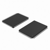
IC FRONT-END MIXED-SGNL 128-LQFP
Manufacturer
Analog Devices Inc
Datasheet
1.AD9860-EBZ.pdf
(32 pages)
Specifications of AD9862BSTRL
Rohs Status
RoHS non-compliant
Rf Type
LMDS, MMDS
Features
12-bit ADC(s), 14-bit DAC(s)
Package / Case
128-LQFP


AD9860/AD9862
default, this bit is low, setting up the DLL in “slow” mode. This
bit must be set high for DLL output frequencies over 64 MHz.
REGISTER 25: CLKOUT
BIT 7, 6: CLKOUT2 Divide Factor
These bits control what rate the CLKOUT2 Pin will operate at
relative to the DLL output rate. The DLL output rate can be
output directly or divided by 2, 4, or 8. Bit 7 is the MSB and
Bit 6 is the LSB.
BIT 5, 1: Inv 2/Inv 1
The output clocks from CLKOUT1 and CLKOUT2 can be
inverted by setting the appropriate one of these bits high.
BIT 4, 0: Dis 2/Dis 1
The output clocks from CLKOUT1 and CLKOUT2 can be
disabled and a logic low output is forced by setting the appro-
priate one of these bits high.
REGISTER 26–33: AUXILIARY ADC A2/A1/B2/B1
AUX ADC A2, A1, B2, B1 Data
These registers are read only registers that are used for read
back of the 10-bit auxiliary ADC. The 10 bits are broken into a
two registers, one containing the upper eight bits and the other
containing the lower two bits.
REGISTER 34: AUX ADC CONTROL
BIT 7: Aux SPI (Enable)
One of the Auxiliary ADCs can be controlled through an dedi-
cated Auxiliary Serial Port. Setting this bit high enables this mode.
BIT 6: Sel BnotA
If the auxiliary Serial port is used, this bit selects which Auxiliary
ADC, A or B, will be using the dedicated Auxiliary Serial port.
The Auxiliary Serial port by default (low setting) controls Auxil-
iary ADC A. Setting this bit high will allow the Auxiliary Serial
Port to control Auxiliary ADC B.
BIT 5, 2: Refsel B/A
By default, the auxiliary ADCs use an external reference applied to
the AUX_REF pin. This voltage will act as the full-scale reference
for the selected auxiliary ADC. Either auxiliary ADC can use an
internally generated reference, which is a buffered version of the
analog supply voltage. To enable use of the internal reference for
either of the auxiliary ADCs, the respective Refsel register should
be set high.
BIT 4, 1: Select B/A
These bits select which of the two inputs will be connected to the
respective auxiliary ADC. By default (setting low), the AUX_ADC_A2
pin is connected to Auxiliary ADC A and AUX_ADC_B2 pin is
connected to Auxiliary ADC B. Setting the respective bit high
will connect the AUX_ADC_A1 pin to Auxiliary ADC A and/or
AUX_ADC_B1 pin to Auxiliary ADC B.
BIT 3, 0: Start B/A
Setting a high bit to either of these registers initiates a conversion
of the respective auxiliary ADC, A or B. The register bit always
reads back a low.
REGISTER 35: AUX ADC CLOCK
BIT 0: CLK/4
By default (setting low), the auxiliary ADCs are run at the receive
ADC conversion rate divided by 2. Setting this bit high will run
MSB, LSB
00 (Default)
01
10
11
Relative CLKOUT2 Frequency
Equals DLL output rate
Equals DLL output rate divided by 2
Equals DLL output rate divided by 4
Equals DLL output rate divided by 8
–16–
the Auxiliary ADCs with a clock that is 1/4 of the receive ADC
conversion rate. The conversion rate of the auxiliary ADCs
should be less than 20 MHz.
REGISTER 36, 37, 38: AUX DAC A/B/C
Auxiliary DAC A, B, and C Output Control Word
Three 8-bit, straight binary words are used to control the output
of three on-chip auxiliary DACs. The auxiliary DAC output
changes take effect immediately after any of the serial write is
completed. The DAC output control words have default values
of 0. The smaller programmed output controlled words corre-
spond to lower DAC output levels.
REGISTER 39: AUX DAC UPDATE
BIT 7: Slave Enable
A low setting (default) updates the auxiliary DACs after the respec-
tive register is written to. To synchronize the auxiliary DAC outputs
to each other, a slave mode can be enabled by setting this bit
high and then setting a high to the appropriate update registers.
BIT 2/1/0: Update C, B, and A
Setting a high bit to any of these registers initiates an update of the
respective Auxiliary DAC, A, B, or C, when Slave mode is enabled
using the Slave Enable register. The register bit is a one shot
and always reads back a low. Note: be sure to keep the Slave Enable
bit high when using the auxiliary DAC synchronization option.
REGISTER 40: AUX DAC POWER-DOWN
BIT 2/1/0: Power Down C, B, and A
Setting any of these bits high will power down the appropriate
auxiliary DAC. By default, these bits are low and the auxiliary
DACs are enabled.
REGISTER 41: AUX DAC CONTROL
BIT 4, 2, 0: Inv C, B, and A
Setting any of these bits high will invert the appropriate Auxiliary
DAC control word setting. By default, these bits are low and the
output control word is decoded as noninverted, straight binary.
REGISTER 42/43: SIGDELT (SIGMA-DELTA)
Sigma-Delta Output Control Word
A 12-bit straight binary word is used to control the output of an
on-chip sigma-delta converter. The sigma-delta output changes
take effect immediately after any serial write is completed. The
sigma-delta output control words have default values of 0. The
smaller programmed output controlled words correspond to lower
integrated sigma-delta output levels.
REGISTER 49,50 : RX LOW POWER MODE
Setting these bits will scale down the bias current to the ADC
analog block when the device is operated at lower speeds. By
default, these bits are low and the bias is at a nominal setting.
For ADC operation at or below 32 MSPS, Register 49 can be set
to 0x03 and Register 50 can be set to 0xEC; this will reduce Rx
AVDD power consumption by about 30% relative to nominal.
For ADC operation at or below 16 MSPS, Register 49 can be set
to 0x03 and Register 50 can be set to 0x9E; this will reduce Rx
AVDD power consumption by about 60% relative to nominal.
REGISTER 63: CHIP ID
BIT 7–0: Rev ID
This read only register indicates the revision of the AD9860/AD9862.
Reserved Registers
Reserved registers are held for future development and should
never be written to.
REV. 0
Related parts for AD9862BSTRL
Image
Part Number
Description
Manufacturer
Datasheet
Request
R

Part Number:
Description:
BOARD EVALUATION FOR AD9862
Manufacturer:
Analog Devices Inc
Datasheet:

Part Number:
Description:
±1.7g Dual-Axis IMEMS Accelerometer Evaluation Board
Manufacturer:
Analog Devices Inc
Datasheet:
Part Number:
Description:
Inertial Sensor Evaluation System
Manufacturer:
Analog Devices Inc
Datasheet:
Part Number:
Description:
Manufacturer:
Analog Devices Inc
Datasheet:
Part Number:
Description:
Manufacturer:
Analog Devices Inc
Datasheet:
Part Number:
Description:
Manufacturer:
Analog Devices Inc
Datasheet:
Part Number:
Description:
Manufacturer:
Analog Devices Inc
Datasheet:
Part Number:
Description:
Manufacturer:
Analog Devices Inc
Datasheet:
Part Number:
Description:
Manufacturer:
Analog Devices Inc
Datasheet:
Part Number:
Description:
Manufacturer:
Analog Devices Inc
Datasheet:
Part Number:
Description:
Manufacturer:
Analog Devices Inc
Datasheet:
Part Number:
Description:
Manufacturer:
Analog Devices Inc
Datasheet:
Part Number:
Description:
Manufacturer:
Analog Devices Inc
Datasheet: