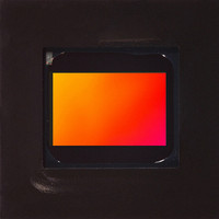
MT9V022IA7ATM Aptina LLC, MT9V022IA7ATM Datasheet

MT9V022IA7ATM
Specifications of MT9V022IA7ATM
Available stocks
Related parts for MT9V022IA7ATM
MT9V022IA7ATM Summary of contents
Page 1
Wide-VGA CMOS Digital Image Sensor Rugged Specs and High Quality for Scene-Understanding and Smart Imaging Applications Micron’s MT9V022 has specifi- cally been designed to support the demanding interior and exterior needs of automotive imaging, which makes it ideal for ...
Page 2
General Description The MT9V022 active imaging pixel array is 752H x 480V. It incorporates sophisticated camera functions on-chip, such as averaging and improve SNR when oper- ating in smaller resolutions, as well as ...
Page 3
In slave mode, the sensor accepts both external integration and readout controls. The integration time is programmed through the two-wire serial interface during master or snapshot modes, or controlled via an externally generated control signal during slave mode. LVDS Serial ...
Page 4
Figure 3: Pixel Array Description and Color Pattern Detail 8 dark, 1 light dummy rows 26 dark, 1 light dummy columns (782,492) 2 dummy rows Output Data Format The MT9V022 image data can be read out in a progressive scan ...
Page 5
Output Data Timing The data output of the MT9V022 is synchronized with the PIXCLK output. When LINE_VALID is HIGH, one 10-bit pixel datum is output every PIXCLK period. Figure 5: Row Timing and FRAME_VALID/LINE_VALID Signals FRAME_VALID LINE_VALID Number of master ...
Page 6
High Dynamic Range The MT9V022 pixel light response can be optionally configured to achieve intra-scene dynamic range as high as 100dB. High dynamic range is achieved by controlling the slopes of a three-segment, piecewise, linear pixel response, as illustrated in ...
Page 7
Automatic Gain Control (AGC) and Automatic Exposure Control (AEC) The integrated AEC/AGC unit is responsible for ensuring that optimal auto settings of exposure and (analog) gain are computed and updated every frame. When the AGC or AEC are enabled, the ...
Page 8
Pixel Binning In addition to windowing mode— in which smaller resolution (CIF, QCIF, user-selected size frame) is obtained by selecting a small window from the sensor array—the MT9V022 provides the ability to show the entire image captured by the pixel ...
Page 9
Table 2: DC Electrical Characteristics (continued 3.3V ±0.3V; T PWR Symbol Definition V LVDS power supply LVDS I LVDS supply current LVDS I A Analog standby supply current PWR Standby I D Digital standby supply current PWR Standby ...
Page 10
Table 4: Absolute Maximum Ratings Symbol V SUPPLY I SUPPLY I GND OUT Note: T STG Note: Stresses greater than those listed may cause permanent damage to the device. This is a stress rating only, and functional ...
Page 11
Figure 12: Quantum Efficiency – Color and Monochrome Figure 13: Typical Configuration (Connection) – Parallel Output Mode Master Clock STANDBY from Controller or Digital GND Two-Wire Serial Interface Note: LVDS signals are to be left floating. PDF:09005aef8201ffc3/Source: 09005aef81ff2525 MT9V022_Product_Brief - ...
Page 12
Figure 14: 52-Ball IBGA Package A LVDS LVDS B BYPASS C _CLKIN SER_ D DATAIN Table 5: Ball Descriptions Only pins D 0 through D OUT 52-Ball IBGA Numbers Symbol H7 RSVD ...
Page 13
Table 5: Ball Descriptions (continued) Only pins D 0 through D OUT 52-Ball IBGA Numbers Symbol A5 SYSCLK G4 S DATA G3 STLN_OUT G5 STFRM_OUT H2 LINE_VALID G2 FRAME_VALID OUT OUT ...
Page 14
Figure 15: 52-Ball IBGA Package Outline Drawing B SEATING PLANE A 0.10 A (FOR REFERENCE ONLY) 7.00 52X Ø0.55 1.00 TYP DIMENSIONS APPLY TO SOLDER BALLS BALL A8 POST REFLOW. THE PRE-REFLOW DIAMETER IS 0.50. 3.50 7.00 1.00 TYP C ...
Page 15
... Ordering Information Production Parts MT9V022I77ATM MT9V022IA7ATM MT9V022I77ATC MT9V022IA7ATC Demo Kits A demonstration kit is also available for evaluation purposes and consists of: • Micron Imaging Demo2 Camera Board • Micron Sensor Head with lens • USB2.0 Cable • Software CD • Demo User Manual picture from Demo Kit ...


