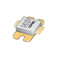
BLF6G10-45 NXP Semiconductors, BLF6G10-45 Datasheet

BLF6G10-45
Specifications of BLF6G10-45
Available stocks
Related parts for BLF6G10-45
BLF6G10-45 Summary of contents
Page 1
... BLF6G10-45 Power LDMOS transistor Rev. 02 — 20 January 2010 1. Product profile 1.1 General description 45 W LDMOS power transistor for base station applications at frequencies from 700 MHz to 1000 MHz. Table 1. RF performance at T Mode of operation 2-carrier W-CDMA [1] Test signal: 3GPP; test model 1; 64 DPCH; PAR = 7 0.01 % probability on CCDF per carrier; carrier spacing 5 MHz ...
Page 2
... Limiting values Parameter Conditions drain-source voltage gate-source voltage drain current storage temperature junction temperature Thermal characteristics Parameter thermal resistance from junction to case Rev. 02 — 20 January 2010 BLF6G10-45 Power LDMOS transistor Simplified outline Symbol 1 [ Min - −0.5 - −65 - ...
Page 3
... RF performance at V class-AB production test circuit. Symbol η D ACPR 7.1 Ruggedness in class-AB operation The BLF6G10-45 is capable of withstanding a load mismatch corresponding to VSWR = through all phases under the following conditions 350 mA BLF6G10-45_2 Product data sheet Characteristics C per section; unless otherwise specified. drain-source breakdown voltage ...
Page 4
... BLF6G10-45_2 Product data sheet (dB 001aah528 70 η D (%) IMD η (dBc − (W) L (PEP) = 960 MHz; 1 Fig 3. Rev. 02 — 20 January 2010 BLF6G10-45 Power LDMOS transistor 001aah527 75 η D (%) η ( −30 −60 − 350 mA 960 MHz 960.1 MHz. 2 Intermodulation distortion as a function of peak envelope load power; typical values ...
Page 5
... BLF6G10-45_2 Product data sheet 001aah530 16 η D (%) 12 (1) ( (dBm) L(AV) = 952.5 MHz; 1 Fig 5. Rev. 02 — 20 January 2010 BLF6G10-45 Power LDMOS transistor −40 ACPR (dBc) −45 (1) (2) −50 −55 − 350 mA 952.5 MHz 957.5 MHz; carrier spacing 5 MHz 955 MHz ...
Page 6
V GG C10 input 50 Ω Fig 6. Test circuit for operation at 900 MHz C9 C11 C12 C13 C14 C15 C16 R2 F1 output C7 50 Ω 001aah532 ...
Page 7
... Figure 7). Value 3 6 1.0 pF 6 330 nF 4.5 μ 220 μ 4.7 Ω; 0.1 W 6.8 Ω; 0.1 W Rev. 02 — 20 January 2010 BLF6G10-45 Power LDMOS transistor − C16 C15 C14 C6 C7 001aah533 = 3.5 and thickness = 0.76 mm. r Remarks [1] [1] [1] [1] [1] [1] ...
Page 8
... REFERENCES JEDEC EIAJ Rev. 02 — 20 January 2010 BLF6G10-45 Power LDMOS transistor 1.70 20.45 9.91 15.24 0.25 0.51 1 ...
Page 9
... MHz from 800 MHz. lower frequency range extended to 700 MHz from 800 MHz. export control disclaimer added. Product data sheet Rev. 02 — 20 January 2010 BLF6G10-45 Power LDMOS transistor Change notice Supersedes - BLF6G10-45_1 - - © NXP B.V. 2010. All rights reserved ...
Page 10
... Export might require a prior authorization from national authorities. 12.4 Trademarks Notice: All referenced brands, product names, service names and trademarks are the property of their respective owners. http://www.nxp.com salesaddresses@nxp.com Rev. 02 — 20 January 2010 BLF6G10-45 Power LDMOS transistor © NXP B.V. 2010. All rights reserved ...
Page 11
... Please be aware that important notices concerning this document and the product(s) described herein, have been included in section ‘Legal information’. © NXP B.V. 2010. For more information, please visit: http://www.nxp.com For sales office addresses, please send an email to: salesaddresses@nxp.com All rights reserved. Date of release: 20 January 2010 Document identifier: BLF6G10-45_2 ...


