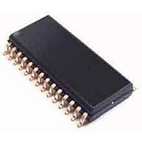
CS8420-DSR Cirrus Logic Inc, CS8420-DSR Datasheet - Page 31

CS8420-DSR
Manufacturer Part Number
CS8420-DSR
Description
Audio DSPs IC Digital Audio Sample Rate Convertr
Manufacturer
Cirrus Logic Inc
Datasheet
1.CS8420-CSZ.pdf
(94 pages)
Specifications of CS8420-DSR
Lead Free Status / RoHS Status
Lead free / RoHS Compliant
DS245F4
9.2
9.3
I²C Mode
In I²C mode, SDA is a bidirectional data line. Data is clocked into and out of the part by the clock, SCL, with
the clock to data relationship as shown in
unique address. Pins AD[1:0] form the two least significant bits of the chip address and should be connected
to VD+ or DGND as desired. The EMPH pin is used to set the AD2 bit, by connecting a resistor from the
EMPH pin to VD+ or to DGND. The state of the pin is sensed while the CS8420 is being reset. The upper
four bits of the 7-bit address field are fixed at 0010b. To communicate with a CS8420, the chip address field,
which is the first byte sent to the CS8420, should match 0010b followed by the settings of the EMPH, AD1,
and AD0. The eighth bit of the address is the R/W bit. If the operation is a write, the next byte is the Memory
Address Pointer (MAP) which selects the register to be read or written. If the operation is a read, the con-
tents of the register pointed to by the MAP will be output. Setting the auto-increment bit in MAP allows suc-
cessive reads or writes of consecutive registers. Each byte is separated by an acknowledge bit. The ACK
bit is output from the CS8420 after each input byte is read and is input to the CS8420 from the microcon-
troller after each transmitted byte.
Interrupts
The CS8420 has a comprehensive interrupt capability. The INT output pin is intended to drive the interrupt
input pin on the host microcontroller. The INT pin may be set to be active-low, active-high, or active-low with
no active pull-up transistor. This last mode is used for active-low, wired-OR hook-ups, with multiple periph-
erals connected to the microcontroller interrupt input pin.
Many conditions can cause an interrupt, as listed in the interrupt status register descriptions. Each source
may be masked via mask registers. In addition, each source may be set to rising-edge, falling-edge, or level-
sensitive. Combined with the option of level-sensitive or edge-sensitive modes within the microcontroller,
many different set-ups are possible, depending on the needs of the equipment designer.
SDA
SCL
Notes:
1. AD2 is derived from a resistor attached to the EMPH pin
2. If operation is a write, this byte contains the Memory Address Pointer, MAP.
3. If operation is a read, the last bit of the read should be NACK (high).
Start
AD1, and AD0 are determined by the state of the corresponding pins.
0010
Figure 23. Control Port Timing in
AD2-0
Note 1
R/W
Figure
ACK DATA7-0 ACK DATA7-0 ACK
23. There is no CS pin. Each individual CS8420 is given a
Note 2
I²C
Mode
Note 3
Stop
CS8420
31


