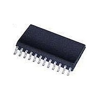
PCK351D NXP Semiconductors, PCK351D Datasheet

PCK351D
Specifications of PCK351D
Available stocks
Related parts for PCK351D
PCK351D Summary of contents
Page 1
PCK351 clock distribution device with 3-state outputs Rev. 02 — 16 December 2005 1. General description The PCK351 is a high-performance 3.3 V LVTTL clock distribution device. The PCK351 enables a single clock input to be distributed ...
Page 2
... MHz output frequency in MHz output load capacitance in pF Ordering information Table +85 C amb Type number PCK351D PCK351DB PCK351_2 Product data sheet clock distribution device with 3-state outputs Quick reference data = 3.0 ns. amb r f Conditions LOW-to-HIGH A input to Yn outputs; propagation delay pF HIGH-to-LOW A input to Yn outputs ...
Page 3
Philips Semiconductors 5. Functional diagram Fig 1. Logic diagram of PCK351 PCK351_2 Product data sheet clock distribution device with 3-state outputs 002aaa282 Rev. 02 — 16 December 2005 PCK351 ...
Page 4
... Rev. 02 — 16 December 2005 PCK351 1 GND Y10 PCK351DB GND 7 8 GND GND 002aaa281 Fig 3. Pin configuration for SSOP24 Description ground (0 V) outputs supply voltage output enable input (active LOW) data input © Koninklijke Philips Electronics N.V. 2005. All rights reserved. ...
Page 5
Philips Semiconductors 7. Functional description Refer to 7.1 Function table Table HIGH voltage level LOW voltage level high-impedance OFF-state 7.2 Logic symbol Fig 4. Logic symbol PCK351_2 Product data sheet ...
Page 6
Philips Semiconductors 8. Limiting values Table 5: In accordance with the Absolute Maximum Rating System (IEC 60134). Symbol O(sink GND T stg P [1] The performance ...
Page 7
Philips Semiconductors 10. Characteristics Table 7: Static characteristics Over recommended operating conditions; voltages are referenced to GND (ground = 0 V). T Symbol Parameter V input clamping voltage IK V HIGH-state output voltage OH V LOW-state output voltage OL I ...
Page 8
Philips Semiconductors Table 8: Dynamic characteristics GND = 2.5 ns Symbol Parameter amb L t LOW-to-HIGH propagation delay PLH t ...
Page 9
Philips Semiconductors Table 9: Switching characteristics Temperature and V coefficients over recommended operating free-air temperature and V CC Symbol Parameter t temperature coefficient of LOW-to-HIGH propagation delay PLH( (average value) t temperature coefficient of HIGH-to-LOW propagation delay ...
Page 10
Philips Semiconductors Fig 7. Calculation of t PCK351_2 Product data sheet clock distribution device with 3-state outputs A input Y1 output t PHL(A-Y1) Y2 output t PHL(A-Y2) Y3 output t PHL(A-Y3) Y4 output t PHL(A-Y4) Y5 output ...
Page 11
Philips Semiconductors 11. Test information Fig 8. Load circuitry for switching times Table 10: Test PLH PHL PLZ PZL PHZ PZH PCK351_2 Product data sheet clock distribution device ...
Page 12
Philips Semiconductors 12. Package outline SO24: plastic small outline package; 24 leads; body width 7 pin 1 index 1 e DIMENSIONS (inch dimensions are derived from the original mm dimensions) A UNIT ...
Page 13
Philips Semiconductors SSOP24: plastic shrink small outline package; 24 leads; body width 5 pin 1 index 1 DIMENSIONS (mm are the original dimensions) A UNIT max. 0.21 1. ...
Page 14
Philips Semiconductors 13. Soldering 13.1 Introduction to soldering surface mount packages This text gives a very brief insight to a complex technology. A more in-depth account of soldering ICs can be found in our Data Handbook IC26; Integrated Circuit Packages ...
Page 15
Philips Semiconductors – smaller than 1.27 mm, the footprint longitudinal axis must be parallel to the transport direction of the printed-circuit board. The footprint must incorporate solder thieves at the downstream end. • For packages with leads on four sides, ...
Page 16
Philips Semiconductors [4] These packages are not suitable for wave soldering. On versions with the heatsink on the bottom side, the solder cannot penetrate between the printed-circuit board and the heatsink. On versions with the heatsink on the top side, ...
Page 17
Philips Semiconductors 15. Data sheet status [1] Level Data sheet status Product status I Objective data Development II Preliminary data Qualification III Product data Production [1] Please consult the most recently issued data sheet before initiating or completing a design. ...
Page 18
Philips Semiconductors 20. Contents 1 General description . . . . . . . . . . . . . . . . . . . . . . 1 2 Features . . . . . . . . ...


