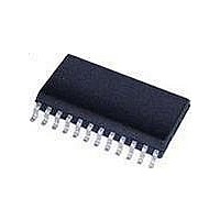
PCK351D NXP Semiconductors, PCK351D Datasheet - Page 5

PCK351D
Manufacturer Part Number
PCK351D
Description
Clock Buffer 1:10 CLK DISTR DEV 3-ST OUTPUT
Manufacturer
NXP Semiconductors
Datasheet
1.PCK351D112.pdf
(18 pages)
Specifications of PCK351D
Number Of Outputs
10
Propagation Delay (max)
4.1 ns
Supply Voltage (max)
3.6 V
Supply Voltage (min)
3 V
Maximum Power Dissipation
650 mW
Maximum Operating Temperature
+ 85 C
Minimum Operating Temperature
- 40 C
Mounting Style
SMD/SMT
Package / Case
SO-24
Operating Supply Voltage (max)
3.6V
Operating Temp Range
-40C to 85C
Propagation Delay Time
6.3ns
Operating Supply Voltage (min)
3V
Mounting
Surface Mount
Pin Count
24
Operating Supply Voltage (typ)
3.3V
Package Type
SO
Quiescent Current
25mA
Power Dissipation
650mW
Operating Temperature Classification
Industrial
Lead Free Status / RoHS Status
Lead free / RoHS Compliant
Other names
PCK351D,112
Available stocks
Company
Part Number
Manufacturer
Quantity
Price
Company:
Part Number:
PCK351DB,112
Manufacturer:
Maxim
Quantity:
49
Philips Semiconductors
7. Functional description
PCK351_2
Product data sheet
7.1 Function table
7.2 Logic symbol
Refer to
Table 4:
H = HIGH voltage level; L = LOW voltage level; Z = high-impedance OFF-state
Fig 4. Logic symbol
Figure 1 “Logic diagram of
A
H
H
L
L
Function table
Inputs
Rev. 02 — 16 December 2005
OE
H
H
L
L
OE
A
1 : 10 clock distribution device with 3-state outputs
5
6
PCK351”.
EN
002aaa283
23
21
19
18
16
14
11
9
4
2
Y1
Y2
Y3
Y4
Y5
Y6
Y7
Y8
Y9
Y10
© Koninklijke Philips Electronics N.V. 2005. All rights reserved.
Outputs
Yn
H
Z
Z
L
PCK351
5 of 18


