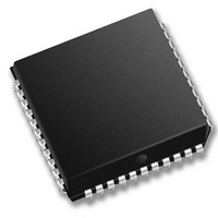
DG884DN Vishay, DG884DN Datasheet - Page 13

DG884DN
Manufacturer Part Number
DG884DN
Description
Video Switch ICs 8x4 Video Crosspoint 18
Manufacturer
Vishay
Datasheet
1.DG884DN-E3.pdf
(14 pages)
Specifications of DG884DN
Supply Voltage (max)
21 V
Supply Voltage (min)
0.3 V
Package / Case
PLCC-44
Mounting Style
SMD/SMT
Lead Free Status / RoHS Status
Lead free / RoHS Compliant
Available stocks
Company
Part Number
Manufacturer
Quantity
Price
Company:
Part Number:
DG884DN
Manufacturer:
SIL
Quantity:
5 510
Part Number:
DG884DN
Manufacturer:
VISHAY/威世
Quantity:
20 000
Company:
Part Number:
DG884DN-E3
Manufacturer:
VISHAY
Quantity:
301
APPLICATIONS
A typical switching threshold versus V
These devices feature an address readback facility whereby
the last address written to the device may be read by the
system. This allows improved status monitoring and hand
shaking without additional external components.
When the I/O assigns the address output condition, the A
address pins can sink or source current for logic low and
high, respectively. Note that V
condition. This point must be respected if V
input logic threshold shifting.
Note: Even though these devices are designed to be latchup
resistant, V
operation or during power supply on/off sequencing.
Vishay Siliconix maintains worldwide manufacturing capability. Products may be manufactured at one of several qualified locations. Reliability data for Silicon
Technology and Package Reliability represent a composite of all qualified locations. For related documents such as package/tape drawings, part marking, and
reliability data, see
Document Number: 70071
S-71241–Rev. H, 25-Jun-07
L
In Bus
In Bus
Video
Video
must not exceed V+ by more than 0.3 V in
http://www.vishay.com/ppg?70071.
L
is the logic high output
Out Bus
Out Bus
Video
Video
L
is shown in Figure 15.
Figure 16. 16 X 8 Expandable Crosspoint Matrix Using DG884
L
is varied for
X
Layout
The PLCC package pinout is optimized so that large
crosspoint arrays can be easily implemented with a minimum
number of PCB layers (see Figure 16). Crosstalk is
minimized and off-isolation is optimized by having ground
pins located adjacent to each input and output signal pins.
Optimum off-isolation and low crosstalk performance can
only be achieved by the proper use of RF layout techniques:
avoid sockets, use ground planes, avoid ground loops,
bypass the power supplies with high frequency type
capacitors (low ESR, low ESL), use striplines to maintain
transmission line impedance matching.
Out Bus
Out Bus
Video
Video
Vishay Siliconix
In Bus
In Bus
Video
Video
www.vishay.com
DG884
13


