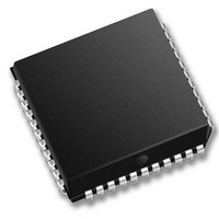
DG884DN Vishay, DG884DN Datasheet - Page 7

DG884DN
Manufacturer Part Number
DG884DN
Description
Video Switch ICs 8x4 Video Crosspoint 18
Manufacturer
Vishay
Datasheet
1.DG884DN-E3.pdf
(14 pages)
Specifications of DG884DN
Supply Voltage (max)
21 V
Supply Voltage (min)
0.3 V
Package / Case
PLCC-44
Mounting Style
SMD/SMT
Lead Free Status / RoHS Status
Lead free / RoHS Compliant
Available stocks
Company
Part Number
Manufacturer
Quantity
Price
Company:
Part Number:
DG884DN
Manufacturer:
SIL
Quantity:
5 510
Part Number:
DG884DN
Manufacturer:
VISHAY/威世
Quantity:
20 000
Company:
Part Number:
DG884DN-E3
Manufacturer:
VISHAY
Quantity:
301
TIMING DIAGRAMS
Document Number: 70071
S-71241–Rev. H, 25-Jun-07
PARAMETER DEFINITIONS
Device A
Device B
Address
Address
Device A
Device B
B
A
CS for
CS for
Address
Address
CS for
CS for
B
A
0
0
SALVO
SALVO
0
0
B
A
WR
B
A
WR
RS
1
3
I/O
I/O
RS
1
3
Symbol
T
T
T
T
T
T
T
T
T
T
T
T
Output
T
T
AW
CW
WC
WA
WP
WS
SW
AO
CO
SP
RS
CA
IA
IO
Input
Reset Occuring at Any Time Results In All Current Event Latches Being Cleared
t
CA
t
IA
t
IO
t
CW
Select Output 1
t
O
t
C
AW
Select Input
Chip Select to WR
WR to Chip Select
Address to Output
I/O to Address In
CS to Address In
Address to Write
Write to Address
t
WP
WR to SALVO
SALVO to WR
SALVO Pulse
RS to SALVO
I/O to Output
CS to Output
Select Current
Event Latch 1
t
Parameter
AO
WR Pulse
Presetting Device A
Address Output 1
t
WA
Interrogating Device A
t
AO
t
Select Output 2
AW
Select Input
Figure 2. Output Timing Requirements
Figure 1. Input Timing Requirements
t
Minimum time address must be valid before WR goes high
Minimum time address must remain valid after WR pulse goes high
Minimum time of WR pulse width to write address into Next Event latches
Minimum time chip select must be valid before a WR pulse
Minimum time chip select must remain valid after WR pulse
Minimum time of SALVO pulse width
Minimum time from WR pulse to SALVOto load new address
Minimum time from SALVO pulse to WR to load current address
Minimum time I/O must be valid before address applied
Minimum time RS must be valid before SALVO pulse
Minimum time I/O must be valid before address output valid
Minimum time address B
Minimum time CS must be valid until A
Minimum time CS must be valid before address applied if I/O is high
WC
t
WA
Reset Occuring at Any Time Results In All Current Event Latches Being Cleared
t
WS
Out N
Latch N
t
CA
t
SP
t
O
C
X
t
Interrogating Device B
SW
must be valid until address A
t AO
Select Current
Event Latch
t
CW
Presetting Device B
t
Address Output
AW
Description
Output N
Input
X
output is valid
t
WA
t
AO
t
WS
t
A
t
C
IA
Vishay Siliconix
X
output valid
t
SP
t
RS
Donít Care
Donít Care
www.vishay.com
DG884
t
SW
7


