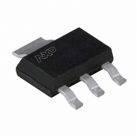
PHT6NQ10T,135 NXP Semiconductors, PHT6NQ10T,135 Datasheet - Page 2

PHT6NQ10T,135
Manufacturer Part Number
PHT6NQ10T,135
Description
MOSFET N-CH 100V 6.5A SOT223
Manufacturer
NXP Semiconductors
Series
TrenchMOS™r
Datasheet
1.PHT6NQ10T135.pdf
(7 pages)
Specifications of PHT6NQ10T,135
Package / Case
SOT-223 (3 leads + Tab), SC-73, TO-261
Fet Type
MOSFET N-Channel, Metal Oxide
Fet Feature
Standard
Rds On (max) @ Id, Vgs
90 mOhm @ 3A, 10V
Drain To Source Voltage (vdss)
100V
Current - Continuous Drain (id) @ 25° C
6.5A
Vgs(th) (max) @ Id
4V @ 1mA
Gate Charge (qg) @ Vgs
21nC @ 10V
Input Capacitance (ciss) @ Vds
633pF @ 25V
Power - Max
8.3W
Mounting Type
Surface Mount
Minimum Operating Temperature
- 65 C
Configuration
Single Dual Drain
Transistor Polarity
N-Channel
Resistance Drain-source Rds (on)
0.09 Ohm @ 10 V
Drain-source Breakdown Voltage
100 V
Gate-source Breakdown Voltage
+/- 20 V
Continuous Drain Current
3 A
Power Dissipation
1800 mW
Maximum Operating Temperature
+ 150 C
Mounting Style
SMD/SMT
Lead Free Status / RoHS Status
Lead free / RoHS Compliant
Lead Free Status / RoHS Status
Lead free / RoHS Compliant, Lead free / RoHS Compliant
Other names
934055876135
PHT6NQ10T /T3
PHT6NQ10T /T3
PHT6NQ10T /T3
PHT6NQ10T /T3
Available stocks
Company
Part Number
Manufacturer
Quantity
Price
Part Number:
PHT6NQ10T,135
Manufacturer:
NEXPERIA/安世
Quantity:
20 000
Philips Semiconductors
ELECTRICAL CHARACTERISTICS
T
REVERSE DIODE LIMITING VALUES AND CHARACTERISTICS
T
August 1999
N-channel TrenchMOS
SYMBOL PARAMETER
V
V
R
I
I
Q
Q
Q
t
t
t
t
L
L
C
C
C
SYMBOL PARAMETER
I
I
V
t
Q
j
j
= 25˚C unless otherwise specified
GSS
DSS
d on
r
d off
f
S
SM
rr
= 25˚C unless otherwise specified
d
s
(BR)DSS
GS(TO)
SD
DS(ON)
iss
oss
rss
g(tot)
gs
gd
rr
Drain-source breakdown
voltage
Gate threshold voltage
Drain-source on-state
resistance
Gate source leakage current V
Zero gate voltage drain
current
Total gate charge
Gate-source charge
Gate-drain (Miller) charge
Turn-on delay time
Turn-on rise time
Turn-off delay time
Turn-off fall time
Internal drain inductance
Internal source inductance
Input capacitance
Output capacitance
Feedback capacitance
Continuous source current
(body diode)
Pulsed source current (body
diode)
Diode forward voltage
Reverse recovery time
Reverse recovery charge
transistor
CONDITIONS
V
V
V
V
I
V
V
Resistive load
Measured tab to centre of die
Measured from source lead to source
bond pad
V
CONDITIONS
T
I
I
V
D
F
F
sp
GS
DS
GS
GS
DS
DD
GS
GS
GS
= 6 A; V
= 6 A; V
= 6 A; -dI
= 25 ˚C
= 0 V; I
= V
= 10 V; I
= 10 V; V
= 100 V; V
= 50 V; R
= 10 V; R
= 0 V; V
= 0 V; V
GS
; I
DD
GS
D
D
F
DS
/dt = 100 A/ s;
R
= 80 V; V
D
= 0 V
= 0.25 mA;
= 1 mA
D
G
= 25 V
= 3 A
GS
2
DS
= 25 V; f = 1 MHz
= 8.2 ;
= 5.6
= 0 V
= 0 V;
GS
= 10 V
T
T
T
T
T
j
j
j
j
j
= 150˚C
= 150˚C
= 150˚C
= -55˚C
= -55˚C
MIN.
MIN.
100
1.2
89
2
-
-
-
-
-
-
-
-
-
-
-
-
-
-
-
-
-
-
-
-
-
-
-
TYP. MAX. UNIT
TYP. MAX. UNIT
0.05
Product specification
633
103
135
2.5
8.2
2.5
0.8
57
10
21
15
20
10
61
55
3
6
5
-
-
-
-
-
-
-
PHT6NQ10T
216
100
500
5.5
1.2
90
10
26
4
6
-
-
-
-
-
-
-
-
-
-
-
-
-
-
-
-
-
Rev 1.000
m
m
nA
nC
nC
nC
nH
nH
nC
pF
pF
pF
ns
ns
ns
ns
ns
V
V
V
V
V
A
A
V
A
A


