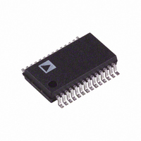
AD9214BRSZ-80 Analog Devices Inc, AD9214BRSZ-80 Datasheet - Page 14

AD9214BRSZ-80
Manufacturer Part Number
AD9214BRSZ-80
Description
ADC Single Pipelined 80MSPS 10-Bit Parallel 28-Pin SSOP
Manufacturer
Analog Devices Inc
Datasheet
1.AD9214BRSZ-RL65.pdf
(20 pages)
Specifications of AD9214BRSZ-80
Package
28SSOP
Resolution
10 Bit
Sampling Rate
80000 KSPS
Architecture
Pipelined
Number Of Analog Inputs
1
Digital Interface Type
Parallel
Input Type
Voltage
Signal To Noise Ratio
58.1(Typ) dB
Polarity Of Input Voltage
Bipolar
Number Of Bits
10
Sampling Rate (per Second)
80M
Data Interface
Parallel
Number Of Converters
1
Power Dissipation (max)
300mW
Voltage Supply Source
Analog and Digital
Operating Temperature
-40°C ~ 85°C
Mounting Type
Surface Mount
Package / Case
28-SSOP (0.200", 5.30mm Width)
Lead Free Status / RoHS Status
Lead free / RoHS Compliant
Available stocks
Company
Part Number
Manufacturer
Quantity
Price
Part Number:
AD9214BRSZ-80
Manufacturer:
ADI/亚德诺
Quantity:
20 000
AD9214
Reference Circuit
The evaluation board is configured at assembly to use the
AD9214’s on-board reference. To supply an external reference,
the user must connect the REFSENSE pin to VCC by removing
the jumper block connecting E25 to E26, and placing it between
E19 and E24. In this configuration, an external 1.25 V reference
must be connected to jumper connection E23. Jumper connections
E19–E21, E24, and resistors R13–R14 are omitted at assembly,
and not used in the evaluation of the AD9214.
Gain/Data Format
The evaluation board is assembled with the DFS/GAIN pin
connected to ground; this configures the AD9214 for a 1 V p-p
analog input range, and offset binary data format. The user may
remove this jumper and replace it to make one of the connections
described in the table below to configure the AD9214 for different
gain and output data format options.
DFS/GAIN
Jumper
Placement
E18 to E12
E16 to E11
E15 to E14
E17 to E13
Power-Down
The evaluation board is configured at assembly so that the
PWRDN input floats low for normal operating condition. The
user may add a jumper between option holes E5 and E6 to
connect PWRDN to AVCC, configuring the AD9214 for power-
down mode.
Encode Signal and Distribution
The encode input signal should drive SMB connector J5, which
has an on-board 50 Ω termination. A standard CMOS compatible
pulse source is recommended. Alternatively, the user can adjust
the dc level of an ac-coupled clock source by adding resistor
R11, normally omitted. J5 drives the AD9214 ENCODE input
and one gate of U12, which buffers and distributes the clock
signal to the on-board latch (U3), the reconstruction DAC
(U11), and the output data connector (U2). The board comes
assembled with timing options optimized for the DAC and latch;
the user may invert the DR signal at Pin 37 of edge connector
U2 by removing the jumper block between E34 and E35, and
reinstalling it between E35 and E36.
Table III. Data Format and Gain Configuration for
Evaluation Board
DFS/GAIN
Connection
AGND
AV
REF
Floating
DD
Differential Output Data
A
1 V p-p
1 V p-p
2 V p-p
2 V p-p
IN
Range
Format
Offset Binary
Two’s Complement
Two’s Complement
Offset Binary
Analog Input
The analog input signal is connected to the evaluation board by
SMB connector J1. As configured at assembly, the signal is ac
coupled by capacitor C10 to transformer T1. This 1:1 transformer
provides a 50 Ω termination for connector J1 via 25 Ω resistors
R1 and R4. T1 also converts the signal at J1 into a differential
signal for the analog inputs of the AD9214. Resistor R3, normally
omitted, can be used to terminate J1 if the transformer is removed.
The user can reconfigure the board to drive the AD9214 single-
endedly by removing the jumper block between E1 and E3, and
replacing it between E3 and E2. In this configuration, capacitor
C2 stabilizes the self-bias of AIN, and resistor R2 provides a
matched impedance for a 50 Ω source at J1.
Transformer T1 can be bypassed by moving the jumper normally
between E40 and E38 to connect E40 to E37, and moving the
jumper normally between E39 and E10 to connect E7 to E10.
In this configuration, the analog input of the AD9214 is driven
single ended, directly from J1; and R3 (normally omitted) should
be installed to terminate any cable connected to J1.
Using the AD8138
An optional driver circuit for the analog input, based on the
AD8138 differential amplifier, is included in the layout of the
AD9214 evaluation board. This portion of the evaluation circuit
is not populated when the board is manufactured, but can be
easily be added by the user. Resistors R5, R16, R18, and R25
are the feedback network that sets the gain of the AD8138.
Resistors R23 and R24 set the common-mode voltage at the
output of the op amp. Resistors R27 and R28, and capacitor
C15, form a low-pass filter at the output of the AD8138, limiting
its noise contribution into the AD9214.
Once the drive circuit is populated, the user should remove the
jumper block normally between E40 and E38, and place it between
E40 and E41. This will ac-couple the analog input signal from
SMB connector J1 to the AD8138 drive circuit. The user will also
need to remove the jumper blocks that normally connect E39 to
E10 and E1 to E3 to remove transformer T1 from the circuit.
DAC Reconstruction Circuit
The data available at output connector U2 is also reconstructed by
DAC U11, the AD9752. This 12-bit, high-speed digital-to-analog
converter is included as a tool in setting up and debugging the
evaluation board. It should not be used to measure the per-
formance of the AD9214, as its performance will not accurately
reflect the performance of the ADC. The DAC’s output, available
at J2, will drive 50 Ω. The user can add a jumper block between
E8 and E9 to activate the SLEEP function of the DAC.


