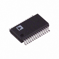
AD9214BRSZ-80 Analog Devices Inc, AD9214BRSZ-80 Datasheet - Page 6

AD9214BRSZ-80
Manufacturer Part Number
AD9214BRSZ-80
Description
ADC Single Pipelined 80MSPS 10-Bit Parallel 28-Pin SSOP
Manufacturer
Analog Devices Inc
Datasheet
1.AD9214BRSZ-RL65.pdf
(20 pages)
Specifications of AD9214BRSZ-80
Package
28SSOP
Resolution
10 Bit
Sampling Rate
80000 KSPS
Architecture
Pipelined
Number Of Analog Inputs
1
Digital Interface Type
Parallel
Input Type
Voltage
Signal To Noise Ratio
58.1(Typ) dB
Polarity Of Input Voltage
Bipolar
Number Of Bits
10
Sampling Rate (per Second)
80M
Data Interface
Parallel
Number Of Converters
1
Power Dissipation (max)
300mW
Voltage Supply Source
Analog and Digital
Operating Temperature
-40°C ~ 85°C
Mounting Type
Surface Mount
Package / Case
28-SSOP (0.200", 5.30mm Width)
Lead Free Status / RoHS Status
Lead free / RoHS Compliant
Available stocks
Company
Part Number
Manufacturer
Quantity
Price
Part Number:
AD9214BRSZ-80
Manufacturer:
ADI/亚德诺
Quantity:
20 000
AD9214
Pin No.
1
2
3
4
5, 8, 11
6, 7, 12
9
10
13
14
15, 23
16, 24
17–22, 25–28
Mnemonic
OR
DFS/GAIN
REFSENSE
REF
AGND
AV
A
AIN
ENCODE
PWRDN
DGND
DrV
D0 (LSB)–D5,
D6–D9 (MSB)
IN
DD
DD
Function
CMOS Output; Out-of-Range Indicator. Logic HIGH indicates the analog input voltage was
outside the converter’s range for the current output data.
Data Format Select and Gain Mode Select. Connect externally to AV
data format and 1 V p-p analog input range. Connect externally to AGND for Offset Binary data
format and 1 V p-p analog input range. Connect externally to REF (Pin 4) for two’s complement
data format and 2 V p-p analog input range. Floating this pin will configure the device for Offset
Binary data format and a 2 V p-p analog input range.
Reference Mode Select Pin for the ADC. This pin is normally connected externally to AGND,
which enables the internal 1.25 V reference, and configures REF (Pin 4) as an analog reference
output pin. Connecting REFSENSE externally to AV
ures REF (Pin 4) as an external reference input. In this case, the user must drive REF with a clean
and accurate 1.25 V (± 5%) reference input.
Reference input or output as configured by REFSENSE (Pin 3). When configured as an output
(REFSENSE = AGND), the internal reference (nominally 1.25 V) is enabled and is available to
the user on this pin. When configured as an input (REFSENSE = AV
REF with a clean and accurate 1.25 V (± 5%) reference. This pin should be bypassed to AGND
with an external 0.1 µF capacitor, whether it is configured as an input or output.
Analog Ground
Analog Power Supply, Nominally 3 V
Positive terminal of the differential analog input for the ADC.
Negative terminal of the differential analog input for the ADC. This pin can be left open if
operating in single-ended mode, but it is preferable to match the impedance seen at the positive
terminal (see Driving the Analog Inputs).
Encode Clock for the ADC. The AD9214 samples the analog signal on the rising edge of ENCODE.
CMOS-compatible power-down mode select, Logic LOW for normal operation; Logic HIGH
for power-down mode (digital outputs in high impedance state). PWRDN has an internal
10 kΩ pull-down resistor to ground.
Digital Output Ground
Digital Output Driver Power Supply. Nominally 2.5 V to 3.6 V.
CMOS Digital Outputs of ADC
28-Lead Shrink Small Outline Package
PIN FUNCTION DESCRIPTIONS
REFSENSE
DFS/GAIN
ENCODE
PWRDN
PIN CONFIGURATION
AGND
AGND
AGND
AV
AV
AV
REF
OR
A
A
DD
DD
DD
IN
IN
10
11
12
13
14
1
2
3
4
5
6
7
8
9
(Not to Scale)
TOP VIEW
AD9214
28
27
26
25
24
23
22
21
20
19
18
17
16
15
D9 (MSB)
D8
D7
D6
DrV
DGND
D5
D4
D3
D2
D1
D0 (LSB)
DrV
DGND
DD
DD
DD
disables the internal reference, and config-
DD
DD
), the user must drive
for two’s complement


