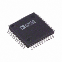
AD6600ASTZ Analog Devices Inc, AD6600ASTZ Datasheet - Page 3

AD6600ASTZ
Manufacturer Part Number
AD6600ASTZ
Description
ADC Single 20MSPS 11-Bit Parallel 44-Pin LQFP
Manufacturer
Analog Devices Inc
Datasheet
1.AD6600ASTZ-REEL.pdf
(24 pages)
Specifications of AD6600ASTZ
Package
44LQFP
Resolution
11 Bit
Sampling Rate
20000 KSPS
Number Of Adcs
1
Number Of Analog Inputs
2
Digital Interface Type
Parallel
Input Type
Voltage
Signal To Noise Ratio
59(Typ) dB
Sample And Hold
Yes
Polarity Of Input Voltage
Bipolar
Number Of Bits
11
Sampling Rate (per Second)
20M
Data Interface
Parallel
Number Of Converters
1
Power Dissipation (max)
976mW
Voltage Supply Source
Single Supply
Operating Temperature
-40°C ~ 85°C
Mounting Type
Surface Mount
Package / Case
44-LQFP
Lead Free Status / RoHS Status
Lead free / RoHS Compliant
Available stocks
Company
Part Number
Manufacturer
Quantity
Price
Company:
Part Number:
AD6600ASTZ
Manufacturer:
Analog Devices Inc
Quantity:
10 000
Part Number:
AD6600ASTZ
Manufacturer:
ADI/亚德诺
Quantity:
20 000
Company:
Part Number:
AD6600ASTZ-REEL
Manufacturer:
Analog Devices Inc
Quantity:
10 000
TIMING REQUIREMENTS AND SWITCHING SPECIFICATIONS
Parameter
A/D CONVERTER
ENCODE INPUTS (ENC, ENC)
2× CLOCK OUTPUT (CLK2×)
OUTPUT RISE/FALL TIMES
NOTES
1
2
3
4
5
6
7
8
Specifications subject to change without notice.
(AVCC = 5 V, DVCC = 3.3 V; ENC and ENC = 20 MSPS; T
Output rise time is measured from 20% point to 80% point of total data voltage swing; output fall time is measured from 80% point to 20% point of total data voltage
See AD6600 Timing Diagrams.
All switching specifications tested by driving ENC and ENC differentially.
Several timing specifications are a function of Encode high time, t
should be kept as close to 50% as possible.
Encode pulse low directly affects the amount of settling time available at FLT resonant port. See External Analog (Resonant) Filter section for details.
The 2× Clock is generated internally, therefore some specifications are functions of encode period and duty cycle. All timing measurements to or from CLK2 × are
referenced to 2.0 V crossing.
This specification IS a function of Encode period and duty cycle; reference timing diagrams Figure 8.
Output rise time is measured from 20% point to 80% point of total CLK2 × voltage swing; output fall time is measured from 80% point to 20% point of total CLK2 ×
voltage swing.
swing. All outputs specified with 10 pF load.
Conversion Rate
Maximum Conversion Rate
Minimum Conversion Rate
Aperture Uncertainty
Period
Pulsewidth High
Pulsewidth Low
Output Frequency
Output Period
CLK2× Pulsewidth Low
Output Risetime
Output Falltime
Output Risetime (D10:D0, RSSI2:0)
Output Falltime (D10:D0, RSSI2:0)
Output Risetime (AB_OUT)
Output Falltime (AB_OUT)
6
4
7
3
7
6
8
5
2
Name
f
t
t
t
t
t
t
t
ENC
j
ENC
ENCH
ENCL
CLK2×_1
CLK2×_2
CLK2×L
MIN
ENCH
= –40 C, T
; these specifications are shown in the data tables and timing diagrams. Encode duty cycle
Temp
Full
Full
25°C
Full
Full
Full
Full
Full
Full
Full
Full
Full
Full
Full
Full
MAX
= +85 C unless otherwise noted.)
Test
Level
II
IV
V
II
IV
IV
V
V
V
V
V
V
V
V
V
50
20
20
Min
20
1
AD6600AST
Typ
1/(t
0.3
2× f
t
t
t
3
2.6
8
8.4
6
6.2
ENCL
ENCH
ENCH
ENC
ENC
/2
)
Max
6
AD6600
Unit
MSPS
MSPS
MSPS
ps rms
ns
ns
ns
MSPS
ns
ns
ns
ns
ns
ns
ns
ns
ns


