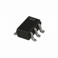
BF1206,115 NXP Semiconductors, BF1206,115 Datasheet - Page 2

BF1206,115
Manufacturer Part Number
BF1206,115
Description
MOSFET N-CH DUAL GATE 6V SOT363
Manufacturer
NXP Semiconductors
Datasheet
1.BF1206115.pdf
(22 pages)
Specifications of BF1206,115
Package / Case
SC-70-6, SC-88, SOT-363
Transistor Type
N-Channel Dual Gate
Frequency
400MHz
Gain
30dB
Voltage - Rated
6V
Current Rating
30mA
Noise Figure
1.3dB
Current - Test
18mA
Voltage - Test
5V
Configuration
Dual Dual Gate
Continuous Drain Current
30 mA
Drain-source Breakdown Voltage
6 V
Maximum Operating Temperature
+ 150 C
Minimum Operating Temperature
- 65 C
Mounting Style
SMD/SMT
Power Dissipation
180 mW
Transistor Polarity
N-Channel
Lead Free Status / RoHS Status
Lead free / RoHS Compliant
Power - Output
-
Lead Free Status / Rohs Status
Lead free / RoHS Compliant
Other names
934057297115
BF1206
BF1206
BF1206
BF1206
NXP Semiconductors
FEATURES
Two low noise gain controlled amplifiers in a single
Superior cross-modulation performance during AGC
High forward transfer admittance
High forward transfer admittance to input capacitance
APPLICATIONS
Gain controlled low noise amplifiers for VHF and UHF
DESCRIPTION
The BF1206 is a combination of two different dual gate
MOS-FET amplifiers with shared source and gate 2 leads.
The source and substrate are interconnected. Internal bias
circuits enable DC stabilization and a very good
cross-modulation performance during AGC. Integrated
diodes between the gates and source protect against
excessive input voltage surges. The transistor is
encapsulated in SOT363 micro-miniature plastic package.
QUICK REFERENCE DATA
2003 Nov 17
Per MOS-FET; unless otherwise specified
V
I
y
C
C
X
NF
D
SYMBOL
package
ratio.
applications with 5 V supply voltage, such as digital and
analog television tuners.
DS
mod
Dual N-channel dual-gate MOS-FET
ig1-s
rss
fs
drain-source voltage
drain current (DC)
forward transfer admittance
input capacitance at gate 1
reverse transfer capacitance
cross-modulation
noise figure
PARAMETER
amp. a: I
amp. b: I
amp. a: I
amp. b: I
f = 1 MHz
amp. a: input level for k = 1% at
40 dB AGC
amp. b: input level for k = 1% at
40 dB AGC
amp. a: f = 400 MHz; I
amp. b: f = 800 MHz; I
amp. a: f = 11 MHz; I
amp. b: f = 11 MHz; I
2
PINNING - SOT363
handbook, halfpage
D
D
D
D
= 18 mA
= 12 mA
= 18 mA; f = 1 MHz
= 12 mA; f = 1 MHz
CONDITIONS
Marking code: L6-.
PIN
1
6
1
2
3
4
5
6
Top view
Fig.1 Simplified outline and symbol.
5
2
D
D
D
D
= 18 mA
= 12 mA
= 18 mA
= 12 mA
4
3
MAM480
drain (b)
source
gate 1 (b)
gate 1 (a)
gate 2
drain (a)
d (b)
d (a)
33
29
102
100
MIN. TYP. MAX. UNIT
DESCRIPTION
AMP
Product specification
a
38
34
2.4
1.7
15
105
103
1.3
1.4
3
3.5
g2
s
BF1206
6
30
48
44
2.9
2.2
1.9
2.0
AMP
b
g1 (a)
g1 (b)
V
mA
mS
mS
pF
pF
fF
dBV
dBV
dB
dB
dB
dB


