PEMT1,115 NXP Semiconductors, PEMT1,115 Datasheet
PEMT1,115
Specifications of PEMT1,115
PEMT1 T/R
PEMT1 T/R


Related parts for PEMT1,115


PEMT1,115 Summary of contents
Page 1
DATA SHEET PEMT1 PNP general purpose double transistor Product data sheet Supersedes data of 2001 Sep 25 DISCRETE SEMICONDUCTORS M3D744 2001 Nov 07 ...
Page 2
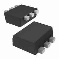
... NXP Semiconductors PNP general purpose double transistor FEATURES • 300 mW total power dissipation • Very small 1.6 × 1.2 mm ultra thin package • Self alignment during soldering due to straight leads • Replaces two SC-75/SC-89 packaged transistors on same PCB area • Reduced required PCB area • ...
Page 3
... NXP Semiconductors PNP general purpose double transistor THERMAL CHARACTERISTICS SYMBOL PARAMETER R thermal resistance from junction to ambient th j-a Notes 1. Transistor mounted on an FR4 printed-circuit board. 2. The only recommended soldering is reflow soldering. CHARACTERISTICS = 25 °C; unless otherwise specified. T amb SYMBOL PARAMETER Per transistor I collector-base cut-off current ...
Page 4
... NXP Semiconductors PNP general purpose double transistor PACKAGE OUTLINE Plastic surface mounted package; 6 leads pin 1 index DIMENSIONS (mm are the original dimensions) UNIT 0.6 0.27 0.18 1.7 mm 0.5 0.17 0.08 1.5 OUTLINE VERSION IEC SOT666 2001 Nov scale 1.3 1.7 0.3 1.0 ...
Page 5
... NXP Semiconductors. In case of any inconsistency or conflict between information in this document and such terms and conditions, the latter will prevail. ...
Page 6
... NXP Semiconductors Customer notification This data sheet was changed to reflect the new company name NXP Semiconductors. No changes were made to the content, except for the legal definitions and disclaimers. Contact information For additional information please visit: http://www.nxp.com For sales offices addresses send e-mail to: salesaddresses@nxp.com © ...