MT48LC16M16A2BG-75:D Micron Technology Inc, MT48LC16M16A2BG-75:D Datasheet - Page 25
MT48LC16M16A2BG-75:D
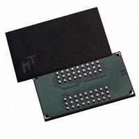
Manufacturer Part Number
MT48LC16M16A2BG-75:D
Description
DRAM Chip SDRAM 256M-Bit 16Mx16 3.3V 54-Pin VFBGA Tray
Manufacturer
Micron Technology Inc
Type
SDRAMr
Specifications of MT48LC16M16A2BG-75:D
Density
256 Mb
Maximum Clock Rate
133 MHz
Package
54VFBGA
Address Bus Width
15 Bit
Operating Supply Voltage
3.3 V
Maximum Random Access Time
6|5.4 ns
Operating Temperature
0 to 70 °C
Format - Memory
RAM
Memory Type
SDRAM
Memory Size
256M (16Mx16)
Speed
133MHz
Interface
Parallel
Voltage - Supply
3 V ~ 3.6 V
Package / Case
54-VFBGA
Organization
16Mx16
Address Bus
15b
Access Time (max)
6/5.4ns
Operating Supply Voltage (typ)
3.3V
Package Type
VFBGA
Operating Temp Range
0C to 70C
Operating Supply Voltage (max)
3.6V
Operating Supply Voltage (min)
3V
Supply Current
135mA
Pin Count
54
Mounting
Surface Mount
Operating Temperature Classification
Commercial
Lead Free Status / RoHS Status
Lead free / RoHS Compliant
Lead Free Status / RoHS Status
Compliant, Lead free / RoHS Compliant
Available stocks
Company
Part Number
Manufacturer
Quantity
Price
Company:

Part Number:
MT48LC16M16A2BG-75:D
Manufacturer:
Micron Technology Inc
Quantity:
10 000
Company:
Part Number:
MT48LC16M16A2BG-75:D TR
Manufacturer:
Micron Technology Inc
Quantity:
10 000


PDF: 09005aef8091e6d1
256Mb_sdr.pdf - Rev. N 1/10 EN
10. Address transitions average one transition every two clocks.
11. PC100 specifies a maximum of 4pF.
12. PC100 specifies a maximum of 5pF.
13. For -75, CL = 3 and tCK = 7.5ns; for -7E, CL = 2 and tCK = 7.5ns.
14. CKE is HIGH during REFRESH command period
5. I
6. I
7. Enables on-chip refresh and address counters.
8. Other input signals are allowed to transition no more than once every two clocks and
9. The I
measured from V
always be 1.5V referenced to crossover. Refer to Micron technical note TN-48-09.
minimum cycle time and the outputs open.
are otherwise at valid V
quency alteration for the test condition.
is actually a nominal value and does not result in a fail value.
DD
DD
specifications are tested after the device is properly initialized.
is dependent on output loading and cycle rates. Specified values are obtained with
DD
current will increase or decrease proportionally according to the amount of fre-
IL, max
and V
IH
25
or V
Electrical Specifications – I
IH,min
IL
levels.
and no longer from the 1.5V midpoint. CLK should
Micron Technology, Inc. reserves the right to change products or specifications without notice.
t
RFC (MIN) else CKE is LOW. The I
256Mb: x4, x8, x16 SDRAM
© 1999 Micron Technology, Inc. All rights reserved.
DD
Parameters
DD6
limit
Related parts for MT48LC16M16A2BG-75:D
Image
Part Number
Description
Manufacturer
Datasheet
Request
R

Part Number:
Description:
IC SDRAM 64MBIT 133MHZ 54TSOP
Manufacturer:
Micron Technology Inc
Datasheet:

Part Number:
Description:
IC SDRAM 64MBIT 5.5NS 86TSOP
Manufacturer:
Micron Technology Inc
Datasheet:
Part Number:
Description:
IC SDRAM 64MBIT 200MHZ 86TSOP
Manufacturer:
Micron Technology Inc
Datasheet:
Part Number:
Description:
IC SDRAM 64MBIT 133MHZ 54TSOP
Manufacturer:
Micron Technology Inc
Datasheet:
Part Number:
Description:
IC SDRAM 128MBIT 133MHZ 54TSOP
Manufacturer:
Micron Technology Inc
Datasheet:

Part Number:
Description:
IC SDRAM 256MBIT 133MHZ 90VFBGA
Manufacturer:
Micron Technology Inc
Datasheet:
Part Number:
Description:
IC SDRAM 128MBIT 133MHZ 54TSOP
Manufacturer:
Micron Technology Inc
Datasheet:
Part Number:
Description:
IC SDRAM 256MBIT 133MHZ 54TSOP
Manufacturer:
Micron Technology Inc
Datasheet:

Part Number:
Description:
IC DDR SDRAM 512MBIT 6NS 66TSOP
Manufacturer:
Micron Technology Inc
Datasheet:
Part Number:
Description:
IC SDRAM 128MBIT 167MHZ 86TSOP
Manufacturer:
Micron Technology Inc
Datasheet:
Part Number:
Description:
IC SDRAM 128MBIT 143MHZ 86TSOP
Manufacturer:
Micron Technology Inc
Datasheet:

Part Number:
Description:
SDRAM 256M-BIT 1.8V 54-PIN VFBGA
Manufacturer:
Micron Technology Inc
Datasheet:
Part Number:
Description:
IC SDRAM 128MBIT 143MHZ 86TSOP
Manufacturer:
Micron Technology Inc
Datasheet:

Part Number:
Description:
IC SDRAM 128MBIT 125MHZ 54VFBGA
Manufacturer:
Micron Technology Inc
Datasheet:
Part Number:
Description:
IC SDRAM 128MBIT 125MHZ 54VFBGA
Manufacturer:
Micron Technology Inc
Datasheet: