MT48LC16M16A2BG-75:D Micron Technology Inc, MT48LC16M16A2BG-75:D Datasheet - Page 68
MT48LC16M16A2BG-75:D
Manufacturer Part Number
MT48LC16M16A2BG-75:D
Description
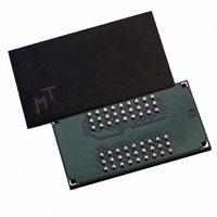
DRAM Chip SDRAM 256M-Bit 16Mx16 3.3V 54-Pin VFBGA Tray
Manufacturer
Micron Technology Inc
Type
SDRAMr
Specifications of MT48LC16M16A2BG-75:D
Density
256 Mb
Maximum Clock Rate
133 MHz
Package
54VFBGA
Address Bus Width
15 Bit
Operating Supply Voltage
3.3 V
Maximum Random Access Time
6|5.4 ns
Operating Temperature
0 to 70 °C
Format - Memory
RAM
Memory Type
SDRAM
Memory Size
256M (16Mx16)
Speed
133MHz
Interface
Parallel
Voltage - Supply
3 V ~ 3.6 V
Package / Case
54-VFBGA
Organization
16Mx16
Address Bus
15b
Access Time (max)
6/5.4ns
Operating Supply Voltage (typ)
3.3V
Package Type
VFBGA
Operating Temp Range
0C to 70C
Operating Supply Voltage (max)
3.6V
Operating Supply Voltage (min)
3V
Supply Current
135mA
Pin Count
54
Mounting
Surface Mount
Operating Temperature Classification
Commercial
Lead Free Status / RoHS Status
Lead free / RoHS Compliant
Lead Free Status / RoHS Status
Compliant, Lead free / RoHS Compliant
Available stocks
Company
Part Number
Manufacturer
Quantity
Price
Company:

Part Number:
MT48LC16M16A2BG-75:D
Manufacturer:
Micron Technology Inc
Quantity:
10 000
Company:
Part Number:
MT48LC16M16A2BG-75:D TR
Manufacturer:
Micron Technology Inc
Quantity:
10 000


Figure 38: WRITE – DQM Operation
Burst Read/Single Write
PDF: 09005aef8091e6d1
256Mb_sdr.pdf - Rev. N 1/10 EN
Command
BA0, BA1
Address
DQM
CKE
CLK
A10
DQ
t CMS
t CKS
t AS
t AS
t AS
ACTIVE
Bank
T0
Row
Row
t CKH
t CMH
t AH
t AH
t AH
Note:
t RCD
t CK
The burst read/single write mode is entered by programming the write burst mode bit
(M9) in the mode register to a 1. In this mode, all WRITE commands result in the access
of a single column location (burst of one), regardless of the programmed burst length.
READ commands access columns according to the programmed burst length and se-
quence, just as in the normal mode of operation (M9 = 0).
T1
NOP
1. For this example, BL = 4.
Disable auto precharge
Enable auto precharge
t CMS
t CL
t DS
Column m
WRITE
T2
Bank
D
t CMH
IN
t DH
t CH
T3
NOP
68
t DS
T4
NOP
Micron Technology, Inc. reserves the right to change products or specifications without notice.
D
IN
t DH
t DS
256Mb: x4, x8, x16 SDRAM
T5
NOP
D
IN
t DH
© 1999 Micron Technology, Inc. All rights reserved.
NOP
T6
WRITE Operation
NOP
T7
Don’t Care
Related parts for MT48LC16M16A2BG-75:D
Image
Part Number
Description
Manufacturer
Datasheet
Request
R

Part Number:
Description:
IC SDRAM 64MBIT 133MHZ 54TSOP
Manufacturer:
Micron Technology Inc
Datasheet:

Part Number:
Description:
IC SDRAM 64MBIT 5.5NS 86TSOP
Manufacturer:
Micron Technology Inc
Datasheet:
Part Number:
Description:
IC SDRAM 64MBIT 200MHZ 86TSOP
Manufacturer:
Micron Technology Inc
Datasheet:
Part Number:
Description:
IC SDRAM 64MBIT 133MHZ 54TSOP
Manufacturer:
Micron Technology Inc
Datasheet:
Part Number:
Description:
IC SDRAM 128MBIT 133MHZ 54TSOP
Manufacturer:
Micron Technology Inc
Datasheet:

Part Number:
Description:
IC SDRAM 256MBIT 133MHZ 90VFBGA
Manufacturer:
Micron Technology Inc
Datasheet:
Part Number:
Description:
IC SDRAM 128MBIT 133MHZ 54TSOP
Manufacturer:
Micron Technology Inc
Datasheet:
Part Number:
Description:
IC SDRAM 256MBIT 133MHZ 54TSOP
Manufacturer:
Micron Technology Inc
Datasheet:

Part Number:
Description:
IC DDR SDRAM 512MBIT 6NS 66TSOP
Manufacturer:
Micron Technology Inc
Datasheet:
Part Number:
Description:
IC SDRAM 128MBIT 167MHZ 86TSOP
Manufacturer:
Micron Technology Inc
Datasheet:
Part Number:
Description:
IC SDRAM 128MBIT 143MHZ 86TSOP
Manufacturer:
Micron Technology Inc
Datasheet:

Part Number:
Description:
SDRAM 256M-BIT 1.8V 54-PIN VFBGA
Manufacturer:
Micron Technology Inc
Datasheet:
Part Number:
Description:
IC SDRAM 128MBIT 143MHZ 86TSOP
Manufacturer:
Micron Technology Inc
Datasheet:

Part Number:
Description:
IC SDRAM 128MBIT 125MHZ 54VFBGA
Manufacturer:
Micron Technology Inc
Datasheet:
Part Number:
Description:
IC SDRAM 128MBIT 125MHZ 54VFBGA
Manufacturer:
Micron Technology Inc
Datasheet: