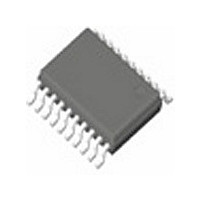
8737-11PGI8 IDT, Integrated Device Technology Inc, 8737-11PGI8 Datasheet - Page 2

8737-11PGI8
Manufacturer Part Number
8737-11PGI8
Description
Manufacturer
IDT, Integrated Device Technology Inc
Type
Clock Dividerr
Datasheet
1.8737-11PGI8.pdf
(12 pages)
Specifications of 8737-11PGI8
Number Of Clock Inputs
2
Mode Of Operation
Differential
Output Frequency
650MHz
Output Logic Level
LVCMOS/LVPECL/LVTTL
Operating Supply Voltage (min)
3.135V
Operating Supply Voltage (typ)
3.3V
Operating Supply Voltage (max)
3.465V
Package Type
TSSOP
Operating Temp Range
-40C to 85C
Operating Temperature Classification
Industrial
Mounting
Surface Mount
Pin Count
20
Lead Free Status / RoHS Status
Not Compliant
PIN CONFIGURATION
PIN DESCRIPTION
NOTE:
1. Pullup and Pulldown refer to internal input resistors. See Capacitance table for typical values.
IDT8737-11
LOW SKEW, ÷ ÷ ÷ ÷ ÷ 1/÷ ÷ ÷ ÷ ÷ 2 DIFFERENTIAL-TO-3.3V LVPECL
xQB1, QB1
xQB0, QB0
xQA1, QA1
xQA0, QA0
CLK_SEL
CLK_EN
Symbol
xPCLK
xCLK
PCLK
CLK
V
V
N C
MR
CLK_SEL
DD
EE
CLK_EN
xPCLK
PCLK
xCLK
CLK
V
V
MR
NC
DD
EE
Number
10, 13, 18
11, 12
14, 15
16, 17
19, 20
1
2
3
4
5
6
7
8
9
1
2
3
4
5
6
7
8
9
10
TOP VIEW
TSSOP
(1)
Unused
Power
Power
Output
Output
Output
Output
Input
Input
Input
Input
Input
Input
Input
20
19
18
17
16
15
14
13
12
11
Type
QA0
xQA0
V
QA1
xQA1
QB0
xQB0
V
QB1
xQB1
Pulldown
Pulldown
Pulldown
Pulldown
DD
DD
Pullup
Pullup
Pullup
2
ABSOLUTE MAXIMUM RATINGS
CAPACITANCE
NOTE:
1. Stresses beyond those listed under ABSOLUTE MAXIMUM RATINGS may cause
R
Parameter
Symbol
V
V
V
θ
T
Negative Supply Pin
Synchronizing Clock Enable. When HIGH, clock outputs follow clock input. When
LOW, Q outputs are forced LOW, xQ outputs are forced HIGH. LVTTL / LVCMOS
interface levels.
Clock Select Input. When HIGH, selects PCLK / xPCLK inputs. When LOW, selects
CLK / xCLK inputs. LVTTL / LVCMOS interface levels.
Inverting Differential Clock Input
Non-Inverting Differential LVPECL Clock Input
Inverting Differential LVPECL Clock Input
No Connection
Master Reset. Resets the output divider. LVTTL / LVCMOS interface levels.
Positive Supply Pins
Differential Output Pair. LVTTL / LVCMOS interface levels.
Differential Output Pair. LVTTL / LVCMOS interface levels.
Differential Output Pair. LVTTL / LVCMOS interface levels.
Differential Output Pair. LVTTL / LVCMOS interface levels.
Non-Inverting Differential Clock Input
R
PULLDOWN
STG
DD
I
O
JA
permanent damage to the device. These are stress ratings only, and functional
operation of the device at these or any other conditions above those indicated in the
operational sections of this specification is not implied. Exposure to absolute-
maximum-rated conditions for extended periods may affect device reliability.
PULLUP
C
IN
COMMERCIAL AND INDUSTRIAL TEMPERATURE RANGES
Power Supply Voltage
Input Voltage
Output Voltage
Package Thermal Impedance (0 lfpm)
Storage Temperature
Description
Input Capacitance
Input Pullup Resistor
Input Pulldown Resistor
Description
(T
A
= +25°C, f = 1MHz, V
Description
Typ.
–0.5 to V
–0.5 to V
—
51
51
–65 to +150
IN
= 0V)
Max
92.6
4.6
DD
DD
Max.
—
—
4
(1)
+0.5
+0.5
°C/W
Unit
Unit
K Ω
K Ω
° C
pF
V
V
V


