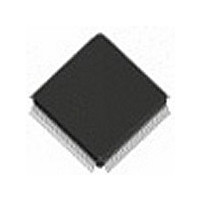
IDT77V1054L25PF IDT, Integrated Device Technology Inc, IDT77V1054L25PF Datasheet - Page 7

IDT77V1054L25PF
Manufacturer Part Number
IDT77V1054L25PF
Description
Manufacturer
IDT, Integrated Device Technology Inc
Datasheet
1.IDT77V1054L25PF.pdf
(29 pages)
Specifications of IDT77V1054L25PF
Data Rate
25.6/51.2Mbps
Number Of Channels
4
Operating Supply Voltage (typ)
3.3V
Operating Supply Voltage (min)
3V
Operating Supply Voltage (max)
3.6V
Operating Temp Range
0C to 70C
Package Type
TQFP
Operating Temperature Classification
Commercial
Mounting
Surface Mount
Lead Free Status / RoHS Status
Not Compliant
Available stocks
Company
Part Number
Manufacturer
Quantity
Price
Company:
Part Number:
IDT77V1054L25PF
Manufacturer:
IDT
Quantity:
297
Transmission Description
transmission begins with the PHY-ATM Interface. An ATM layer
device transfers a cell into the 77V1054 across the Utopia transmit
bus. This cell enters a 3-cell deep transmit FIFO. Once a complete cell
is in the FIFO, transmission begins by passing the cell, four bits (MSB
first) at a time to the 'Scrambler'.
against the 4 high order bits (X(t), X(t-1), X(t-2), X(t-3)) of a 10 bit
pseudo-random nibble generator (PRNG). Its function is to provide the
appropriate frequency distribution for the signal across the line.
of whether the processed nibble is part of a data or command byte.
Note however that only data nibbles are scrambled. The entire
command byte (X _C) is NOT scrambled before it's encoded (see
diagram for illustration). The PRNG is based upon the following
polynomial:
be generated from the following equations:
X(t+1).
time an X_X command is sent. An X_X command is initiated only at
the beginning of a cell transfer after the PRNG has cycled through all
of its states (2
transmitted after power on will also be accompanied with an X_X
command byte. Each time an X_X command byte is sent, the first
nibble after the last escape (X) nibble is XOR'd with 1111b (PRNG =
3FFx).
the possibility of a reset PRNG start-of-cell command and a timing
marker command occurring consecutively does exist (e.g. X_X_X_8).
In this case, the detection of the last two consecutive escape (X)
nibbles will cause the PRNG to reset to its initial 3FFx state. Therefore,
the PRNG is clocked only after the first nibble of the second consecu-
tive escape pair.
nibbles are further encoded using a 4b/5b process. The 4b/5b scheme
ensures that an appropriate number of signal transitions occur on the
line. A total of seventeen 5-bit symbols are used to represent the
sixteen 4-bit data nibbles and the one escape (X) nibble. The table
below lists the 4-bit data with their corresponding 5-bit symbols:
IDT77V1054
Quad Port ATM PHY for 25.6 and 51.2 Mbps with 8-bit Utopia 2
The 'Scrambler' takes each nibble of data and exclusive-ORs them
The PRNG is clocked every time a nibble is processed, regardless
With this polynomial, the four output data bits (D3, D2, D1, D0) will
The following nibble is scrambled with X(t+4), X(t+3), X(t+2), and
A scrambler lock between the transmitter and receiver occurs each
Because a timing marker command (X_8) may occur at any time,
Once the data nibbles have been scrambled using the PRNG, the
Refer to the TC Transmit Block Diagram on the previous page. Cell
10
- 1 = 1023 states). The first valid ATM data cell
X
D3 = d3 xor X(t-3)
D2 = d2 xor X(t-2)
D1 = d1 xor X(t-1)
D0 = d0 xor X(t)
10
+ X
7
+ 1
6.42
7
properties. Among them is the fact that the output data bits can be
represented by a set of relatively simple symbols;
bols whether a timing marker command (X_8) or a start-of-cell com-
mand was sent (X_X or X_4). If a start-of-cell command is detected,
the next 53 bytes received are decoded and forwarded to the
descrambler. (See TC Receive Block Diagram, Figure 3).
encoder. The NRZI code transitions the wire voltage each time a '1' bit
is sent. This, together with the previous encoding schemes guarantees
that long run lengths of either '0' or '1's are prevented. Each symbol is
shifted out with its most significant bit sent first.
Transmit HEC Byte Calculation/Insertion
calculated automatically across the first 4 bytes of the cell header,
depending upon the setting of bit 5 of registers 0x03, 0x13, 0x23 and
0x33. This byte is then either inserted as a replacement of the fifth byte
transferred to the PHY by the external system, or the cell is transmitted
as received. A third operating mode provides for insertion of
"Bad" HEC codes which may aid in communication diagnostics. These
modes are controlled by the LED Driver and HEC Status/Control
Registers.
active by continuing to transmit valid symbols. But it does not transmit
another start-of-cell command until it has another cell for transmission.
The 77V1054 never generates idle cells.
ESC(X) = 00010
• Run length is limited to <= 5;
• Disparity never exceeds +/- 1.
This encode/decode implementation has several very desirable
On the receiver, the decoder determines from the received sym-
The output of the 4b/5b encoder provides serial data to the NRZI
Byte #5 of each ATM cell, the HEC (Header Error Control) is
When no cells are available to transmit, the 77V1054 keeps the line
Data
0010
0110
1010
1110
0000
0100
1000
1100
Data
Symbol
Symbol
01010
01110
11010
11110
10101
00111
10010
10111
0001
0101
1001
1101
Data
0011
0111
1011
1111
Data
Symbol
Symbol
Preliminary
01001
01101
11001
11101
01011
01111
11011
11111
3505 drw 05a
.
.


