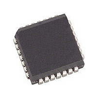
NLXT361PE.A2 S E001 Cortina Systems Inc, NLXT361PE.A2 S E001 Datasheet - Page 11

NLXT361PE.A2 S E001
Manufacturer Part Number
NLXT361PE.A2 S E001
Description
Manufacturer
Cortina Systems Inc
Datasheet
1.NLXT361PE.A2_S_E001.pdf
(55 pages)
Specifications of NLXT361PE.A2 S E001
Number Of Transceivers
1
Operating Supply Voltage (typ)
5V
Screening Level
Industrial
Mounting
Surface Mount
Operating Supply Voltage (min)
4.75V
Operating Supply Voltage (max)
5.25V
Operating Temperature (min)
-40C
Operating Temperature (max)
85C
Lead Free Status / RoHS Status
Not Compliant
Datasheet
1. DI = Digital Input; DO = Digital Output; DI/O = Digital Input/Output; AI = Analog Input; AO = Analog Output.
PLCC
10
11
12
13
16
14
15
17
18
19
20
21
Table 3.
9
Pin #
QFP
10
13
15
19
16
18
20
21
24
25
27
7
9
LXT361 Signal Descriptions (Continued)
Integrated T1/E1 LH/SH Transceiver for DS1/DSX-1 or PRI Applications — LXT361
WR / R/W
Symbol
RRING
RD/DS
TRING
TGND
TVCC
TTIP
RTIP
VCC
AD6
AD7
INT
CS
DI/O
I/O
DO
AO
DI
DI
DI
AI
-
-
-
1
Read. On an Intel bus, driving RD Low commands a LXT361 register read
operation.
Data Strobe. On a Motorola bus, DS goes Low when data is being driven
on the address/data bus. Data is valid on the rising edge of DS.
Address/Data Bus 6 and 7. Used with AD0 - AD5 to form the address/
data bus. Conforms to Intel and Motorola multiplexed address/data bus
specifications.
Write. On an Intel bus, driving WR Low commands a LXT361 register write
operation.
Read/Write. On a Motorola bus, driving R/W High commands a LXT361
register read operation; driving it Low commands a write operation.
Transmit Tip and Ring. Differential driver output pair designed to drive a
50 - 200 Ω load. The transformer and line matching resistors should be
selected to give the desired pulse height and return loss performance. See
“Application Information” on page
Ground return for the transmit driver power supply TVCC.
+5 VDC Power Supply for the transmit drivers. TVCC must not vary from
VCC by more than ± 0.3 V.
Chip Select. During a read or write operation, CS must remain Low. See
Figure 16
In the case of a single processor controlling several chips, this line is used
to select a specific transceiver.
Interrupt. INT goes Low to flag the host when LOS, AIS, NLOOP, QRSS,
DFMS or DFMO bits changes state, or when an elastic store overflow or
underflow occurs. To identify the specific interrupt, read the Performance
Status Register (PSR). To clear or mask an interrupt, write a one to the
appropriate bit in the Interrupt Clear Register (ICR). To re-enable the
interrupt, write a zero. INT is an open drain output that must be
connected to VCC through a pull-up resistor.
Receive Tip and Ring. The Alternate Mark Inversion (AMI) signal received
from the line is applied at these pins. A 1:1 transformer is required. Data
and clock recovered from RTIP/RRING are output on the RPOS/RNEG (or
RDATA in Unipolar mode), and RCLK pins.
+5 VDC Power Supply for all circuits except the transmit drivers. Transmit
drivers are supplied by TVCC.
and
Figure 17
for timing requirements.
Description
32.
11


